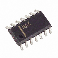
MAX4168ESD+ Maxim Integrated Products, MAX4168ESD+ Datasheet - Page 9

MAX4168ESD+
Manufacturer Part Number
MAX4168ESD+
Description
IC OP AMP R-R I/O W/SD 14-SOIC
Manufacturer
Maxim Integrated Products
Datasheet
1.MAX4166ELAT.pdf
(17 pages)
Specifications of MAX4168ESD+
Amplifier Type
General Purpose
Number Of Circuits
2
Output Type
Rail-to-Rail
Slew Rate
2 V/µs
Gain Bandwidth Product
5MHz
Current - Input Bias
50nA
Voltage - Input Offset
250µV
Current - Supply
1.3mA
Current - Output / Channel
125mA
Voltage - Supply, Single/dual (±)
2.7 V ~ 6.5 V, ±1.35 V ~ 3.25 V
Operating Temperature
-40°C ~ 85°C
Mounting Type
Surface Mount
Package / Case
14-SOIC (3.9mm Width), 14-SOL
Number Of Channels
2
Voltage Gain Db
120 dB
Common Mode Rejection Ratio (min)
72 dB
Input Offset Voltage
0.85 mV
Operating Supply Voltage
3 V, 5 V
Maximum Power Dissipation
667 mW
Maximum Operating Temperature
+ 85 C
Mounting Style
SMD/SMT
Maximum Dual Supply Voltage
+/- 3.25 V
Minimum Operating Temperature
- 40 C
Lead Free Status / RoHS Status
Lead free / RoHS Compliant
-3db Bandwidth
-
Lead Free Status / Rohs Status
Details
Warning: Due to the high output current drive, this op
amp can exceed the absolute maximum power-dissi-
pation rating. As a general rule, as long as the peak cur-
rent is less than or equal to 80mA, the maximum package
power dissipation will not be exceeded for any of the
package types offered. There are some exceptions to this
rule, however. The absolute maximum power-dissipation
rating of each package should always be verified using
the following equations. The following equation gives an
approximation of the package power dissipation:
where: V
For example, the circuit in Figure 1 has a package
power dissipation of 157mW.
Therefore, P
Adding a coupling capacitor improves the package
power dissipation because there is no DC current to
the load, as shown in Figure 2.
High-Output-Drive, Precision, Low-Power, Single-
I
V
Supply, Rail-to-Rail I/O Op Amps with Shutdown
RMS
V
RMS
I
RMS
RMS
I
RMS
RMS
IC(DISS)
I
P
DC
71 84
6 5
IC DISS
I
V
17 67
6 5
DC
.
V
CC
= the RMS voltage from V
= the RMS voltage from V
= the RMS current flowing out of or into
= the phase difference between the
.
.
Applications Information
CC
.
V
+
V
when sourcing current
when sinking current
the op amp and the load
voltage and the current. For resistive
loads, COS
_______________________________________________________________________________________
+
mA
mA
I
Package Power Dissipation
PEAK
= V
= 157mW
I
V
PEAK
3 25
RMS
V
3 25
2
DC
RMS
.
DC
.
RMS
2
V
V
RMS RMS
V
I
RMS
3 25
V
1 5
60
V
.
1 5
0
= 1.
PEAK
I
.
PEAK
.
A
2
2
2
V
COS
2
V
V
COS
1 5
2 189
.
2 189
.
1 5
.
V
.
/
2
V
CC
OUT
60
V
/
V
2
RMS
60
RMS
to V
to V
OUT
EE
Therefore, P
The absolute maximum power-dissipation rating of this
package would be exceeded if the configuration in
Figure 1 were used with all four of the MAX4169ESD’s
amplifiers at a high ambient temperature of +75°C
(157mW x 4 amplifiers = 628mW + a derating of
8.33mW/°C x 5°C = 669mW). Note that 669mW just
exceeds the absolute maximum power dissipation of
667mW for the 14-pin SO package (see the Absolute
Maximum Ratings section).
Figure 1. A Circuit Example where the MAX4165/MAX4166 is
Being Used in Single-Supply Operation
Figure 2. A Circuit Example where Adding a Coupling
Capacitor Greatly Reduces the Power Dissipation of Its
Package
V
C
IN
V
C
IN
= 3Vp-p
=
2 R
= 3Vp-p
1
L
f
L
IC(DISS)
C
C
= V
= 38.6mW
R
R
R
R
RMS
MAX4165
MAX4166
I
MAX4165
MAX4166
RMS
6.5V
6.5V
COS
C
C
60
60
9


