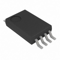
MCP608T-I/ST Microchip Technology, MCP608T-I/ST Datasheet - Page 11

MCP608T-I/ST
Manufacturer Part Number
MCP608T-I/ST
Description
IC OPAMP 2.5V R-R W/CS 8TSSOP
Manufacturer
Microchip Technology
Specifications of MCP608T-I/ST
Slew Rate
0.08 V/µs
Amplifier Type
General Purpose
Number Of Circuits
1
Output Type
Rail-to-Rail
Gain Bandwidth Product
155kHz
Current - Input Bias
1pA
Voltage - Input Offset
250µV
Current - Supply
18.7µA
Current - Output / Channel
17mA
Voltage - Supply, Single/dual (±)
2.5 V ~ 6 V
Operating Temperature
-40°C ~ 85°C
Mounting Type
Surface Mount
Package / Case
8-TSSOP
Op Amp Type
Low Power
No. Of Amplifiers
1
Bandwidth
155kHz
Supply Voltage Range
2.5V To 5.5V
Amplifier Case Style
TSSOP
No. Of Pins
8
Number Of Channels
1
Voltage Gain Db
121 dB
Common Mode Rejection Ratio (min)
75 dB
Input Offset Voltage
0.25 mV
Operating Supply Voltage
3 V, 5 V
Maximum Operating Temperature
+ 85 C
Mounting Style
SMD/SMT
Minimum Operating Temperature
- 40 C
Lead Free Status / RoHS Status
Lead free / RoHS Compliant
-3db Bandwidth
-
Lead Free Status / Rohs Status
Details
Available stocks
Company
Part Number
Manufacturer
Quantity
Price
Company:
Part Number:
MCP608T-I/ST
Manufacturer:
MICROCHIP
Quantity:
12 000
Part Number:
MCP608T-I/ST
Manufacturer:
MICROCHIP/微芯
Quantity:
20 000
4.0
The MCP606/7/8/9 family of op amps is manufactured
using Microchip’s state-of-the-art CMOS process
These op amps are unity-gain stable and suitable for a
wide range of general purpose applications.
4.1
The MCP606/7/8/9 op amps are designed to prevent
phase reversal when the input pins exceed the supply
voltages.
exceeding the supply voltage without any phase rever-
sal.
The inputs of the MCP606/7/8/9 op amps connect to a
differential PMOS input stage. The Common Mode
Input Voltage Range (V
supply systems (V
means that the amplifier input behaves linearly as long
as the Common Mode Input Voltage (V
the specified V
+25°C).
Input voltages that exceed the Absolute Maximum
Voltage Range (V
excessive current to flow into or out of the input pins.
Current beyond ±2 mA can cause reliability problems.
Applications that exceed this rating must be externally
limited with a resistor, as shown in Figure 4-1.
FIGURE 4-1:
Resistor (R
4.2
There are two specifications that describe the output-
swing capability of the MCP606/7/8/9 family of op amps.
The first specification (Maximum Output Voltage Swing)
defines the absolute maximum swing that can be
achieved under the specified load conditions. For
instance, the output voltage swings to within 15 mV of
the negative rail with a 25 k load to V
shows how the output voltage is limited when the input
goes beyond the linear region of operation.
The second specification that describes the output-
swing capability of these amplifiers (Linear Output
Voltage Range) defines the maximum output swing that
can be achieved while the amplifier still operates in its
© 2005 Microchip Technology Inc.
V
IN
APPLICATIONS INFORMATION
Inputs
Rail-to-Rail Output
R
R
IN
Figure 2-23
IN
IN
).
CMR
------------------------------------------------------------------------------
R
V
-------------------------------------------------------------------------- -
Maximum expected V
IN
SS
SS
SS
–
limits (V
), but does not include V
– 0.3V to V
Minimum expected V
Input Current-Limiting
CMR
MCP60X
shows
2 mA
2 mA
) includes ground in single-
SS
– 0.3V to V
DD
the
IN
+ 0.3V) can cause
DD
CM
–
input
/2. Figure 2-23
) is kept within
V
IN
DD
DD
V
OUT
– 1.1V at
DD
voltage
. This
linear region. To verify linear operation in this range, the
large-signal DC Open-Loop Gain (A
points inside the supply rails. The measurement must
meet the specified A
table.
4.3
Driving large capacitive loads can cause stability
problems for voltage-feedback op amps. As the load
capacitance increases, the feedback loop’s phase
margin decreases and the closed-loop bandwidth is
reduced. This produces gain-peaking in the frequency
response, with overshoot and ringing in the step
response. A unity-gain buffer (G = +1) is the most
sensitive to capacitive loads, though all gains show the
same general behavior.
When driving large capacitive loads with these op
amps (e.g., > 60 pF when G = +1), a small series
resistor at the output (R
feedback loop’s phase margin (stability) by making the
output load resistive at higher frequencies. The
bandwidth will be generally lower than the bandwidth
with no capacitive load.
FIGURE 4-2:
stabilizes large capacitive loads.
Figure 4-3 gives recommended R
different capacitive loads and gains. The x-axis is the
normalized load capacitance (C
circuit’s noise gain. For non-inverting gains, G
Signal Gain are equal. For inverting gains, G
1+|Signal Gain| (e.g., -1 V/V gives G
FIGURE 4-3:
for Capacitive Loads.
V
10k
100
1k
IN
10p
10000
1000
100
Capacitive Loads
10
Normalized Load Capacitance; C
MCP60X
MCP606/7/8/9
OL
100p
100
Output Resistor, R
Recommended R
ISO
conditions in the specification
in Figure 4-2) improves the
G
G
G
N
N
N
R
= +1
= +2
C
ISO
L
+4
L
/G
1n
N
OL
1000
), where G
N
DS11177D-page 11
ISO
) is measured at
= +2 V/V).
L
/G
ISO
V
ISO
values for
N
OUT
N
(F)
Values
N
and the
10n
is the
10000
N
is


