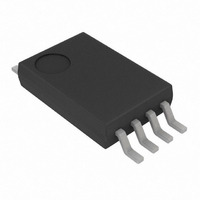
MCP608T-I/ST Microchip Technology, MCP608T-I/ST Datasheet - Page 2

MCP608T-I/ST
Manufacturer Part Number
MCP608T-I/ST
Description
IC OPAMP 2.5V R-R W/CS 8TSSOP
Manufacturer
Microchip Technology
Specifications of MCP608T-I/ST
Slew Rate
0.08 V/µs
Amplifier Type
General Purpose
Number Of Circuits
1
Output Type
Rail-to-Rail
Gain Bandwidth Product
155kHz
Current - Input Bias
1pA
Voltage - Input Offset
250µV
Current - Supply
18.7µA
Current - Output / Channel
17mA
Voltage - Supply, Single/dual (±)
2.5 V ~ 6 V
Operating Temperature
-40°C ~ 85°C
Mounting Type
Surface Mount
Package / Case
8-TSSOP
Op Amp Type
Low Power
No. Of Amplifiers
1
Bandwidth
155kHz
Supply Voltage Range
2.5V To 5.5V
Amplifier Case Style
TSSOP
No. Of Pins
8
Number Of Channels
1
Voltage Gain Db
121 dB
Common Mode Rejection Ratio (min)
75 dB
Input Offset Voltage
0.25 mV
Operating Supply Voltage
3 V, 5 V
Maximum Operating Temperature
+ 85 C
Mounting Style
SMD/SMT
Minimum Operating Temperature
- 40 C
Lead Free Status / RoHS Status
Lead free / RoHS Compliant
-3db Bandwidth
-
Lead Free Status / Rohs Status
Details
Available stocks
Company
Part Number
Manufacturer
Quantity
Price
Company:
Part Number:
MCP608T-I/ST
Manufacturer:
MICROCHIP
Quantity:
12 000
Part Number:
MCP608T-I/ST
Manufacturer:
MICROCHIP/微芯
Quantity:
20 000
MCP606/7/8/9
1.0
Absolute Maximum Ratings †
V
All Inputs and Outputs ................... V
Difference Input Voltage ...................................... |V
Output Short Circuit Current ..................................continuous
Current at Input Pins ....................................................±2 mA
Current at Output and Supply Pins ............................±30 mA
Storage temperature ....................................-65°C to +150°C
Maximum Junction Temperature (T
ESD protection on all pins (HBM;MM) ...................2 kV; 200V
DC CHARACTERISTICS
DS11177D-page 2
Electrical Characteristics: Unless otherwise indicated, V
V
Input Offset
Input Offset Voltage
Input Offset Drift with Temperature
Power Supply Rejection Ratio
Input Bias Current and Impedance
Input Bias Current
Input Offset Bias Current
Common Mode Input Impedance
Differential Input Impedance
Common Mode
Common Mode Input Range
Common Mode Rejection Ratio
Open-Loop Gain
DC Open-Loop Gain
(Large-signal)
DC Open-Loop Gain
(Large-signal)
Output
Maximum Output Voltage Swing
Linear Output Voltage Range
Output Short Circuit Current
Power Supply
Supply Voltage
Quiescent Current per Amplifier
DD
OUT
At Temperature
– V
SS
V
ELECTRICAL
CHARACTERISTICS
DD
.......................................................................7.0V
/2 and R
Parameters
L
= 100 k to V
J
) ......................... +150°C
DD
SS
/2.
– 0.3V to V
V
V
CMRR
V
PSRR
OL
OL
Z
V
V
V
Sym
Z
V
OS
A
A
V
I
I
I
DIFF
CMR
OUT
OUT
I
I
I
OS
SC
SC
CM
, V
, V
DD
OS
OL
OL
Q
B
B
/ T
OH
OH
A
DD
DD
V
V
V
V
V
SS
SS
+ 0.3V
SS
SS
SS
– V
-250
Min
105
100
2.5
80
75
—
—
—
—
—
—
—
—
—
+ 100
– 0.3
+ 15
+ 45
+ 50
SS
DD
|
= +2.5V to +5.5V, V
10
10
18.7
±1.8
Typ
121
118
93
91
17
—
—
—
—
—
—
—
13
13
1
1
7
† Notice: Stresses above those listed under “Absolute
Maximum Ratings” may cause permanent damage to the
device. This is a stress rating only and functional operation of
the device at those or any other conditions above those
indicated in the operational listings of this specification is not
implied. Exposure to maximum rating conditions for extended
periods may affect device reliability.
||6
||6
V
V
V
V
V
DD
DD
DD
DD
DD
+250
SS
Max
5.5
80
25
—
—
—
—
—
—
—
—
—
—
—
– 100
– 1.1
– 20
– 60
– 50
= GND, T
µV/°C T
Units
mV
mV
mV
mV
mA
mA
µV
dB
pA
pA
pA
dB
dB
dB
µA
||pF
||pF
V
V
A
= +25°C, V
© 2005 Microchip Technology Inc.
T
CMRR
V
V
R
V
R
V
R
0.5V output overdrive
R
0.5V output overdrive
R
A
R
A
V
V
I
O
A
A
DD
CM
L
OUT
L
OUT
L
L
L
OL
L
OL
DD
DD
= 0
= -40°C to +85°C
= +85°C
= 25 k to V
= 5 k to V
= 25 k to V
= 5 k
= 25 k
= 5 k
= 5V,
= 2.5V
= 5.5V
= -0.3V to 3.9V
= 50 mV to V
= 0.1V to V
105 dB
100 dB
CM
75 dB
Conditions
to V
to V
= V
to V
DD
DD
DD
DD
DD
DD
DD
DD
/2,
/2,
/2,
/2,
/2,
/2,
/2,
DD
– 0.1V
– 50 mV


