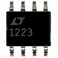
LT1223CS8 Linear Technology, LT1223CS8 Datasheet - Page 11

LT1223CS8
Manufacturer Part Number
LT1223CS8
Description
IC CURRNT FEEDBK AMP100MHZ 8SOIC
Manufacturer
Linear Technology
Datasheet
1.LT1223CN8PBF.pdf
(16 pages)
Specifications of LT1223CS8
Amplifier Type
Current Feedback
Number Of Circuits
1
Slew Rate
1300 V/µs
-3db Bandwidth
100MHz
Current - Input Bias
1µA
Voltage - Input Offset
1000µV
Current - Supply
6mA
Current - Output / Channel
60mA
Voltage - Supply, Single/dual (±)
8 V ~ 36 V, ±4 V ~ 18 V
Operating Temperature
0°C ~ 70°C
Mounting Type
Surface Mount
Package / Case
8-SOIC (3.9mm Width)
Lead Free Status / RoHS Status
Contains lead / RoHS non-compliant
Output Type
-
Gain Bandwidth Product
-
Available stocks
Company
Part Number
Manufacturer
Quantity
Price
Part Number:
LT1223CS8
Manufacturer:
LINEAR/凌特
Quantity:
20 000
Part Number:
LT1223CS8#PBF
Manufacturer:
LINEAR/凌特
Quantity:
20 000
Part Number:
LT1223CS8#TRPBF
Manufacturer:
LINEAR/凌特
Quantity:
20 000
APPLICATIO S I FOR ATIO
Summing Amplifier (DC Accurate)
The summing amplifier is easily made by adding additional
inputs to the basic inverting amplifier configuration. The
LT1223 has no I
between the two input bias currents. Therefore, we will not
improve the DC accuracy of the inverting amplifier by
putting in the extra resistor in the noninverting input.
Difference Amplifier
The LT1223 difference amplifier delivers excellent
performance if the source impedance is very low. This is
because the common mode input resistance is only equal
to R
Video Instrumentation Amplifier
This instrumentation amplifier uses two LT1223s to in-
crease the input resistance to well over 1M. This makes an
excellent “loop through” or cable sensing amplifier if the
F
+ R
V
OUT
V1
V2
G
=
V
V
V
.
I1
I2
In
R
R
G
F
(V1 – V2)
R
R
G
G
R
R
R
G
G
G
OS
•
•
•
1
n
2
U
spec because there is no correlation
(R
F
+
–
V
– 50)
OUT
LT1223
U
+
–
LT1223
= –R
R
F
R
F
F
(
100
V
R
I1
G1
W
+
R
V
LT1223 • TA08
I2
G2
OPTIONAL TRIM
FOR CMRR
LT1223 • TA07
+
V
OUT
R
V
V
In
Gn
OUT
)
U
inverting input (A1) senses the shield and the non-invert-
ing input (A2) senses the center conductor. Since this
amplifier does not load the cable (take care to minimize
stray capacitance) and it rejects common mode hum and
noise, several amplifiers can sense the signal with only
one termination at the end of the cable. The design
equations are simple. Just select the gain you need (it
should be two or more) and the value of the feedback
resistor (typically 1k) and calculate R
can be tweaked with R
The bandwidth of the noninverting input signal is not
reduced by the presence of the other amplifier, however,
the inverting input signal bandwidth is reduced since it
passes two amplifiers. The CMRR is good at high frequen-
cies because the bandwidth of the amplifiers are about the
same even though they do not necessarily operate at the
same gain.
Cable Driver
The cable driver circuit is shown on the front page. When
driving a cable it is important to properly terminate both
ends if even modest high frequency performance is
required. The additional advantage of this is that it isolates
the capacitive load of the cable from the amplifier so it can
operate at maximum bandwidth.
V
R
TRIM GAIN (G) WITH R
OUT
F1
= R
R
1k
= G (V
G1
F2
; R
V
IN
IN
G1
+
–
= (G – 1) R
– V
+
–
IN
LT1223
–
)
A1
G2
R
1k
F1
; TRIM CMRR WITH R
F2
; R
G2
G2
=
G – 1
and the CMRR with R
R
F2
R
1k
G2
G1
V
IN
+
G1
–
+
LT1223
and R
A2
R
1k
F2
LT1223
G1
G2
. The gain
if needed.
11
LT1223 • TA09
1223fb
V
OUT


