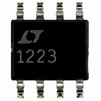
LT1223CS8 Linear Technology, LT1223CS8 Datasheet - Page 8

LT1223CS8
Manufacturer Part Number
LT1223CS8
Description
IC CURRNT FEEDBK AMP100MHZ 8SOIC
Manufacturer
Linear Technology
Datasheet
1.LT1223CN8PBF.pdf
(16 pages)
Specifications of LT1223CS8
Amplifier Type
Current Feedback
Number Of Circuits
1
Slew Rate
1300 V/µs
-3db Bandwidth
100MHz
Current - Input Bias
1µA
Voltage - Input Offset
1000µV
Current - Supply
6mA
Current - Output / Channel
60mA
Voltage - Supply, Single/dual (±)
8 V ~ 36 V, ±4 V ~ 18 V
Operating Temperature
0°C ~ 70°C
Mounting Type
Surface Mount
Package / Case
8-SOIC (3.9mm Width)
Lead Free Status / RoHS Status
Contains lead / RoHS non-compliant
Output Type
-
Gain Bandwidth Product
-
Available stocks
Company
Part Number
Manufacturer
Quantity
Price
Part Number:
LT1223CS8
Manufacturer:
LINEAR/凌特
Quantity:
20 000
Part Number:
LT1223CS8#PBF
Manufacturer:
LINEAR/凌特
Quantity:
20 000
Part Number:
LT1223CS8#TRPBF
Manufacturer:
LINEAR/凌特
Quantity:
20 000
APPLICATIO S I FOR ATIO
The curve on the first page shows the LT1223 voltage gain
versus frequency while driving 100Ω, for five gain settings
from 1 to 100. The feedback resistor is a constant 1k and
the gain resistor is varied from infinity to 10Ω. Shown for
comparison is a plot of the fixed 100MHz gain bandwidth
limitation that a voltage feedback amplifier would have. It
is obvious that for gains greater than one, the LT1223
provides 3 to 20 times more bandwidth. It is also evident
that second order effects reduce the bandwidth somewhat
at the higher gain settings.
Feedback Resistor Selection
Because the feedback resistor determines the compensa-
tion of the LT1223, bandwidth and transient response can
be optimized for almost every application. To increase the
bandwidth when using higher gains, the feedback resistor
(and gain resistor) can be reduced from the nominal 1k
value. The Minimum Feedback Resistor versus Voltage
Gain curve shows the values to use for ±15V supplies.
Larger feedback resistors can also be used to slow down
the LT1223 as shown in the –3dB Bandwidth versus
Feedback Resistor curve.
Capacitive Loads
The LT1223 can be isolated from capacitive loads with a
small resistor (10Ω to 20Ω) or it can drive the capacitive
load directly if the feedback resistor is increased. Both
techniques lower the amplifier’s bandwidth about the
same amount. The advantage of resistive isolation is that
the bandwidth is only reduced when the capacitive load is
present. The disadvantage of resistor isolation is that
resistive loading causes gain errors. Because the DC
accuracy is not degraded with resistive loading, the de-
sired way of driving capacitive loads, such as flash con-
verters, is to increase the feedback resistor. The Maximum
Capacitive Load versus Feedback Resistor curve shows
the value of feedback resistor and capacitive load that
gives 5dB of peaking. For less peaking, use a larger
feedback resistor.
Power Supplies
The LT1223 may be operated with single or split supplies
as low as ±4V (8V total) to as high as ±18V (36V total). It
LT1223
8
U
U
W
U
is not necessary to use equal value split supplies, how-
ever, the offset voltage will degrade about 350µV per volt
of mismatch. The internal compensation capacitor de-
creases with increasing supply voltage. The –3dB Band-
width versus Supply Voltage curve shows how this affects
the bandwidth for various feedback resistors. Generally,
the bandwidth at ±5V supplies is about half the value it is
at ±15V supplies for a given feedback resistor.
The LT1223 is very stable even with minimal supply
bypassing, however, the transient response will suffer if
the supply rings. It is recommended for good slew rate and
settling time that 4.7µF tantalum capacitors be placed
within 0.5 inches of the supply pins.
Input Range
The noninverting input of the LT1223 looks like a 10M
resistor in parallel with a 3pF capacitor until the common
mode range is exceeded. The input impedance drops
somewhat and the input current rises to about 10µA when
the input comes too close to the supplies. Eventually,
when the input exceeds the supply by one diode drop, the
base collector junction of the input transistor forward
biases and the input current rises dramatically. The input
current should be limited to 10mA when exceeding the
supplies. The amplifier will recover quickly when the input
is returned to its normal common mode range unless the
input was over 500mV beyond the supplies, then it will
take an extra 100ns.
Offset Adjust
Output offset voltage is equal to the input offset voltage
times the gain plus the inverting input bias current times
the feedback resistor. For low gain applications (3 or less)
a 10kΩ pot connected to Pins 1 and 5 with wiper to V
trim the inverting input current (±10µA) to null the output;
it does not change the offset voltage very much. If the
LT1223 is used in a high gain application, where input
offset voltage is the dominate error, it can be nulled by
pulling approximately 100µA from Pin 1 or 5. The easy
way to do this is to use a 10kΩ pot between Pin 1 and 5 with
a 150k resistor from the wiper to ground for 15V supply
applications. Use a 47k resistor when operating on a 5V
supply.
+
1223fb
will


