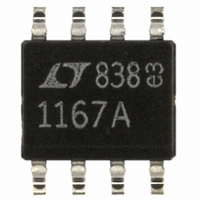
LT1167ACS8#PBF Linear Technology, LT1167ACS8#PBF Datasheet

LT1167ACS8#PBF
Specifications of LT1167ACS8#PBF
Available stocks
Related parts for LT1167ACS8#PBF
LT1167ACS8#PBF Summary of contents
Page 1
... The LT1167, offered in 8-pin PDIP and SO packages, requires significantly less PC board area than discrete multi op amp and resistor designs. These advantages make the LT1167 the most cost effective solution for precision instrumentation amplifier applications. , LTC and LT are registered trademarks of Linear Technology Corporation. Gain Nonlinearity LT1167 1 ...
Page 2
LT1167 ABSOLUTE AXI U RATI GS (Note 1) Supply Voltage ...................................................... 20V Differential Input Voltage (Within the Supply Voltage) ..................................................... 40V Input Voltage (Equal to Supply Voltage) ................ 20V Input Current (Note 3) ........................................ 20mA Output Short-Circuit ...
Page 3
ELECTRICAL CHARACTERISTICS SYMBOL PARAMETER CONDITIONS (Note 7) i Input Noise Current Input Noise Current Density Input Resistance Differential Input Capacitance f IN(DIFF Common Mode Input f IN(CM) O ...
Page 4
LT1167 ELECTRICAL CHARACTERISTICS temperature range, otherwise specifications are at T SYMBOL PARAMETER Gain Error Gain Nonlinearity G/T Gain vs Temperature V Total Input Referred OST Offset Voltage V Input Offset Voltage OSI V Input Offset Voltage Hysteresis OSIH V Output ...
Page 5
ELECTRICAL CHARACTERISTICS The denotes specifications which apply over the full operating temperature range, otherwise specifications are 15V 0V, – Note 1: Absolute Maximum Ratings are ...
Page 6
LT1167 W U TYPICAL PERFOR A CE CHARACTERISTICS Gain Nonlinearity 1167 G01 OUTPUT VOLTAGE (2V/DIV 10V OUT Gain Nonlinearity 1000 1167 G04 OUTPUT VOLTAGE (2V/DIV) G ...
Page 7
W U TYPICAL PERFOR A CE CHARACTERISTICS Distribution of Output Offset Voltage – 137 N8 (2 LOTS 15V S 165 S8 (3 LOTS 302 TOTAL PARTS 30 25 ...
Page 8
LT1167 W U TYPICAL PERFOR A CE CHARACTERISTICS Input Bias Current vs Common Mode Input Voltage 500 400 300 200 100 –100 0 C – 200 25 C – – 300 – 400 ...
Page 9
W U TYPICAL PERFOR A CE CHARACTERISTICS Current Noise Density vs Frequency 1000 V = 15V 100 100 1000 FREQUENCY (Hz) 1167 G22 Overshoot vs Capacitive Load 100 V ...
Page 10
LT1167 W U TYPICAL PERFOR A CE CHARACTERISTICS Undistorted Output Swing vs Frequency 15V 10, 100, 1000 ...
Page 11
W BLOCK DIAGRA + V R3 400 –IN 2 – 400 +IN 3 – V THEORY OF OPERATIO The LT1167 is a modified version of the three op amp instrumentation ...
Page 12
LT1167 THEORY OF OPERATIO Input and Output Offset Voltage The offset voltage of the LT1167 has two components: the output offset and the input offset. The total offset voltage referred to the input (RTI) is found by dividing the output ...
Page 13
THEORY OF OPERATIO – R THERMOCOUPLE LT1167 G + 10k Figure 3. Providing an Input Common Mode Current Path U U APPLICATIO S I FOR ATIO The LT1167 is a low power precision instrumentation amplifier that requires only one external ...
Page 14
LT1167 U U APPLICATIO S I FOR ATIO To significantly reduce the effect of these out-of-band signals on the input offset voltage of instrumentation amplifiers, simple lowpass filters can be used at the inputs. These filters should be located very ...
Page 15
U U APPLICATIO S I FOR ATIO 10V 350 350 R 499 350 350 PRECISION BRIDGE TRANSDUCER Table 1. “Roll Your Own” vs LT1167 Error Budget ERROR SOURCE Absolute Accuracy Input Offset Voltage, V ...
Page 16
LT1167 U U APPLICATIO S I FOR ATIO + LT1167 G REF – 4 –IN – LT1464 V [(+IN) – (–IN)] ...
Page 17
U U APPLICATIO S I FOR ATIO 5V 1 3.5k 3. 200 249 3.5k 3.5k U TYPICAL APPLICATIO –IN + TECHNOLOGIES 67-8-3 R40KQ (0.02% RATIO MATCH 40k LT1167 20k 1 ...
Page 18
LT1167 PACKAGE DESCRIPTION 0.300 – 0.325 (7.620 – 8.255) 0.009 – 0.015 (0.229 – 0.381) +0.035 0.325 –0.015 +0.889 8.255 –0.381 18 U Dimensions in inches (millimeters) unless otherwise noted. N8 Package 8-Lead PDIP (Narrow 0.300) (LTC DWG # 05-08-1510) ...
Page 19
... FLASH SHALL NOT EXCEED 0.010" (0.254mm) PER SIDE Information furnished by Linear Technology Corporation is believed to be accurate and reliable. However, no responsibility is assumed for its use. Linear Technology Corporation makes no represen- tation that the interconnection of its circuits as described herein will not infringe on existing patent rights. ...
Page 20
... Accuracy at Low and High Frequencies, 90MHz GBW, 22V/ s, 900ns Settling Lowpass, Bandpass, Highpass Responses; Low Noise, Low Distortion, Four 2nd Order Filter Sections Single 5V Supply, Bipolar Input Range: 10V, Power Dissipation: 55mW Typ < 105 A S 1167fa LT/TP 0301 2K REV A • PRINTED IN USA LINEAR TECHNOLOGY CORPORATION 1998 ...


