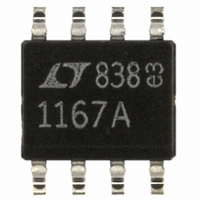
LT1167ACS8#PBF Linear Technology, LT1167ACS8#PBF Datasheet - Page 15

LT1167ACS8#PBF
Manufacturer Part Number
LT1167ACS8#PBF
Description
IC PREC INSTRMNT-AMP PROG 8-SOIC
Manufacturer
Linear Technology
Specifications of LT1167ACS8#PBF
Amplifier Type
Instrumentation
Number Of Circuits
1
Slew Rate
1.2 V/µs
Gain Bandwidth Product
1MHz
Current - Input Bias
50pA
Voltage - Input Offset
15µV
Current - Supply
900µA
Current - Output / Channel
27mA
Voltage - Supply, Single/dual (±)
4.6 V ~ 36 V, ±2.3 V ~ 18 V
Operating Temperature
0°C ~ 70°C
Mounting Type
Surface Mount
Package / Case
8-SOIC (3.9mm Width)
No. Of Amplifiers
1
Input Offset Voltage
15µV
Gain Db Min
1dB
Gain Db Max
10000dB
Bandwidth
1000kHz
Amplifier Output
Single Ended
Cmrr
140dB
Supply Voltage Range
± 2.3V To
Rohs Compliant
Yes
Lead Free Status / RoHS Status
Lead free / RoHS Compliant
Output Type
-
-3db Bandwidth
-
Available stocks
Company
Part Number
Manufacturer
Quantity
Price
APPLICATIO S I FOR ATIO
Table 1. “Roll Your Own” vs LT1167 Error Budget
ERROR SOURCE
Absolute Accuracy at T
Input Offset Voltage, V
Output Offset Voltage, V
Input Offset Current, nA
CMR, dB
Drift to 85 C
Gain Drift, ppm/ C
Input Offset Voltage Drift, V/ C
Output Offset Voltage Drift, V/ C
Resolution
Gain Nonlinearity, ppm of Full Scale
Typ 0.1Hz to 10Hz Voltage Noise, V
G = 100, V
All errors are min/max and referred to input.
Current Source
Figure 7 shows a simple, accurate, low power program-
mable current source. The differential voltage across Pins
2 and 3 is mirrored across R
amplified and applied across R
PRECISION BRIDGE TRANSDUCER
350
350
S
= 15V
10V
350
350
A
= 25 C
U
U
P-P
G
. The voltage across R
499
X
R
, defining the output
W
G
LT1167C CIRCUIT CALCULATION
60 V/20mV
(300 V/100)/20mV
[(450pA)(350/2) ]/20mV
110dB [ 3.16ppm)(5V)]/20mV
(50ppm + 10ppm)(60 C)
[(0.4 V/ C)(60 C)]/20mV
[6 V/ C)(60 C)]/100/20mV
15ppm
0.28 V
LT1167 MONOLITHIC
INSTRUMENTATION AMPLIFIER
G = 100, R
SUPPLY CURRENT = 1.3mA MAX
P-P
+
–
Figure 6. “Roll Your Own” vs LT1167
/20mV
G
LT1167C
= 10ppm TC
U
REF
G
is
current. The 50 A bias current flowing from Pin 5 is
buffered by the LT1464 JFET operational amplifier. This
has the effect of improving the resolution of the current
source to 3pA, which is the maximum I
Replacing R
increases the range of available output currents.
“ROLL YOUR OWN”’ CIRCUIT
100 V/20mV
[(60 V)(2)/100]/20mV
[(450pA)(350 )/2]/20mV
[(0.02% Match)(5V)]/20mV
Total Absolute Error
(100ppm/ C Track)(60 C)
[(1.6 V/ C)(60 C)]/20mV
[(1.1 V/ C)(2)(60 C)]/100/20mV
Total Drift Error
10ppm
(0.3 V
Total Resolution Error
Grand Total Error
CALCULATION
P-P
202 **
)( 2)/20mV
G
+
–
–
+
LT1114A
LT1114A
with a programmable resistor greatly
1/4
1/4
** DISCRETE 1% RESISTOR, 100ppm/ C TC
* 0.02% RESISTOR MATCH, 3ppm/ C TRACKING
“ROLL YOUR OWN” INST AMP, G = 100
100ppm TRACKING
SUPPLY CURRENT = 1.35mA FOR 3 AMPLIFIERS
10k**
10k**
10k*
10k*
LT1167C “ROLL YOUR OWN”
ERROR, ppm OF FULL SCALE
3000
3944
3600
1200
4980
8953
150
790
180
15
14
29
4
–
+
LT1114A
B
1/4
of the LT1464A.
10k*
10k*
LT1167
10866
16461
5000
5564
6000
4800
500
60
66
10
21
31
4
15
1167 F06


