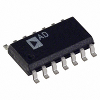
AD824AR-14 Analog Devices Inc, AD824AR-14 Datasheet - Page 14

AD824AR-14
Manufacturer Part Number
AD824AR-14
Description
IC OPAMP JFET R-R 2MHZ LP 14SOIC
Manufacturer
Analog Devices Inc
Datasheet
1.AD824ARZ-14-REEL.pdf
(16 pages)
Specifications of AD824AR-14
Slew Rate
2 V/µs
Rohs Status
RoHS non-compliant
Amplifier Type
J-FET
Number Of Circuits
4
Output Type
Rail-to-Rail
Gain Bandwidth Product
2MHz
-3db Bandwidth
2MHz
Current - Input Bias
4pA
Voltage - Input Offset
500µV
Current - Supply
560µA
Current - Output / Channel
12mA
Voltage - Supply, Single/dual (±)
3 V ~ 30 V, ±1.5 V ~ 15 V
Operating Temperature
-40°C ~ 85°C
Mounting Type
Surface Mount
Package / Case
14-SOIC (3.9mm Width), 14-SOL
Op Amp Type
Low Power
No. Of Amplifiers
4
Bandwidth
2MHz
Supply Voltage Range
3V To 30V
Amplifier Case Style
SOIC
No. Of Pins
14
Operating Temperature Range
-40°C To +85°C
Lead Free Status / RoHS Status
Contains lead / RoHS non-compliant
Available stocks
Company
Part Number
Manufacturer
Quantity
Price
Part Number:
AD824AR-14
Manufacturer:
ADI/亚德诺
Quantity:
20 000
Company:
Part Number:
AD824AR-14-REEL
Manufacturer:
AD
Quantity:
1 240
AD824
A design consideration in sample-and-hold circuits is voltage
droop at the output caused by op amp bias and switch leakage
currents. By choosing a JFET op amp and a low leakage CMOS
switch, this design minimizes droop rate error to better than
0.1 mV/ms in this circuit. Higher values of C
droop rate. For best performance, C
styrene, polypropylene or Teflon capacitors. These types of
capacitors exhibit low leakage and low dielectric absorption. Addi-
tionally, 1% metal film resistors were used throughout the design.
In the sample mode, SW1 and SW4 are closed, and the output
is V
with SW1, is to reduce the pedestal, or hold step, error by
injecting the same amount of charge into the noninverting input
of A3 that SW1 injects into the inverting input of A3. This
creates a common-mode voltage across the inputs of A3 and is
then rejected by the CMR of A3; otherwise, the charge injection
from SW1 would create a differential voltage step error that
would appear at V
OUT
= –V
IN
. The purpose of SW4, which operates in parallel
OUT
. The pedestal error for this circuit is
H
and C2 should be poly-
H
will yield a lower
–14–
less than 2 mV over the entire 0 V to 3.3 V/5 V signal range.
Another method of reducing pedestal error is to reduce the pulse
amplitude applied to the control pins. In order to control the
ADG513, only 2.4 V are required for the “ON” state and
0.8 V for the “OFF” state. If possible, use an input control
signal whose amplitude ranges from 0.8 V to 2.4 V instead of a
full range 0 V to 3.3 V/5 V for minimum pedestal error.
Other circuit features include an acquisition time of less than
3 ms to 1%; reducing C
time further, but an increased pedestal error will result. Settling
time is less than 300 ns to 1%, and the sample-mode signal BW
is 80 kHz.
The ADG513 was chosen for its ability to work with 3 V/5 V
supplies and for having normallyopen and normallyclosed preci-
sion CMOS switches on a dielectrically isolated process. SW2 is
not required in this circuit; however, it was used in parallel with
SW3 to provide a lower R
H
and C2 will speed up the acquisition
ON
analog switch.
REV. C


