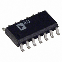
AD824AR-14 Analog Devices Inc, AD824AR-14 Datasheet - Page 5

AD824AR-14
Manufacturer Part Number
AD824AR-14
Description
IC OPAMP JFET R-R 2MHZ LP 14SOIC
Manufacturer
Analog Devices Inc
Datasheet
1.AD824ARZ-14-REEL.pdf
(16 pages)
Specifications of AD824AR-14
Slew Rate
2 V/µs
Rohs Status
RoHS non-compliant
Amplifier Type
J-FET
Number Of Circuits
4
Output Type
Rail-to-Rail
Gain Bandwidth Product
2MHz
-3db Bandwidth
2MHz
Current - Input Bias
4pA
Voltage - Input Offset
500µV
Current - Supply
560µA
Current - Output / Channel
12mA
Voltage - Supply, Single/dual (±)
3 V ~ 30 V, ±1.5 V ~ 15 V
Operating Temperature
-40°C ~ 85°C
Mounting Type
Surface Mount
Package / Case
14-SOIC (3.9mm Width), 14-SOL
Op Amp Type
Low Power
No. Of Amplifiers
4
Bandwidth
2MHz
Supply Voltage Range
3V To 30V
Amplifier Case Style
SOIC
No. Of Pins
14
Operating Temperature Range
-40°C To +85°C
Lead Free Status / RoHS Status
Contains lead / RoHS non-compliant
Available stocks
Company
Part Number
Manufacturer
Quantity
Price
Part Number:
AD824AR-14
Manufacturer:
ADI/亚德诺
Quantity:
20 000
Company:
Part Number:
AD824AR-14-REEL
Manufacturer:
AD
Quantity:
1 240
WAFER TEST LIMITS
Parameter
Offset Voltage
Input Bias Current
Input Offset Current
Input Voltage Range
Common-Mode Rejection Ratio
Power Supply Rejection Ratio
Large Signal Voltage Gain
Output Voltage High
Output Voltage Low
Supply Current/Amplifier
NOTE
Electrical tests and wafer probe to the limits shown. Due to variations in assembly methods and normal yield loss, yield after packaging is not guaranteed for
standard product dice. Consult factory to negotiate specifications based on dice lot qualifications through sample lot assembly and testing.
ABSOLUTE MAXIMUM RATINGS
Supply Voltage . . . . . . . . . . . . . . . . . . . . . . . . . . . . . . . . ± 18 V
Input Voltage . . . . . . . . . . . . . . . . . . . . . . . –V
Differential Input Voltage . . . . . . . . . . . . . . . . . . . . . . . ± 30 V
Output Short Circuit Duration to GND . . . . . . . . . Indefinite
Storage Temperature Range
Operating Temperature Range
Junction Temperature Range
Lead Temperature Range (Soldering 60 sec) . . . . . . . . . 300∞C
Package Type
14-Lead SOIC (R)
16-Lead SOIC (R)
NOTES
1
2
Model
AD824AR-14
AD824AR-14-3V –40∞C to +85∞C 14-Pin SOIC
AD824AR-16
REV. C
CAUTION
ESD (electrostatic discharge) sensitive device. Electrostatic charges as high as 4000 V readily
accumulate on the human body and test equipment and can discharge without detection. Although
the AD824 features proprietary ESD protection circuitry, permanent damage may occur on devices
subjected to high-energy electrostatic discharges. Therefore, proper ESD precautions are
recommended to avoid performance degradation or loss of functionality.
Absolute maximum ratings apply to packaged parts unless otherwise noted.
q
for P-DIP packages; q
package.
JA
R-14, R-16 Packages . . . . . . . . . . . . . . . . –65∞C to +150∞C
AD824A . . . . . . . . . . . . . . . . . . . . . . . . . . . –40∞C to +85∞C
R-14, R-16 Packages . . . . . . . . . . . . . . . . –65∞C to +150∞C
is specified for the worst case conditions, i.e., q
Temperature
Range
–40∞C to +85∞C 14-Pin SOIC
–40∞C to +85∞C 16-Pin SOIC
JA
is specified for device soldered in circuit board for SOIC
ORDERING GUIDE
(@ V
q
120
92
JA
Package
Description
S
2
= 5.0 V, V
1
JA
is specified for device in socket
CM
V
I
I
V
CMRR
PSRR
A
V
V
I
q
36
27
Symbol
B
OS
SY
JC
OS
CM
VO
OH
OL
= 0 V, T
S
– 0.2 V to +V
Package
Option
R-14
R-14
R-16
A
= 25 C unless otherwise noted)
Unit
∞C/W
∞C/W
S
–5–
Conditions
V
V = + 2.7 V to +12 V
R
I
I
V
SOURCE
SINK
CM
L
O
+IN
–IN
= 2 kW
= 0 V, R
R13
= 0 V to 2 V
= 20 mA
R1
J1
= 20 mA
Figure 1. Simplified Schematic of 1/4 AD824
I1
R12
J2
L
R15
R2
= •
Q4
Q2
Q8
R14
I2
Q5
Q3
R9
Q6
I3
Limit
1.0
12
20
–0.2 to 3.0
66
70
15
4.975
25
600
V
V
CC
EE
C2
C3
Q7
WARNING!
I4
I5
C1
Q19
Q22
Q24 Q25
Q21 Q27
R7
ESD SENSITIVE DEVICE
R17
I6
Q20
Q23
Q31
AD824
Q28
Q18
Unit
mV max
pA max
pA
V min
dB min
mV/V
V/mV min
V min
mV max
mA max
C4
Q26
Q29
V
OUT


