EL5421CYZ Intersil, EL5421CYZ Datasheet
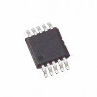
IC BUFFER QUAD R-R 12MHZ 10-MSOP

EL5421CYZ

Manufacturer Part Number
EL5421CYZ
Description
IC BUFFER QUAD R-R 12MHZ 10-MSOP
Manufacturer
Intersil
Datasheet

Specifications of EL5421CYZ

Amplifier Type
Buffer
Number Of Circuits
4
Output Type
Rail-to-Rail
Slew Rate
10 V/µs
-3db Bandwidth
12MHz
Current - Input Bias
2nA
Voltage - Input Offset
2000µV
Current - Supply
500µA
Current - Output / Channel
120mA
Voltage - Supply, Single/dual (±)
4.5 V ~ 16.5 V, ±2.25 V ~ 8.25 V
Operating Temperature
-40°C ~ 85°C
Mounting Type
Surface Mount
Package / Case
10-MSOP, Micro10™, 10-uMAX, 10-uSOP
Lead Free Status / RoHS Status
Lead free / RoHS Compliant
Gain Bandwidth Product
-

Available stocks

Company
Part Number
Manufacturer
Quantity
Price
Part Number:
EL5421CYZ
Manufacturer:
ST
Quantity:
1 200
Part Number:
EL5421CYZ
Manufacturer:
INTERSIL
Quantity:
20 000
Part Number:
EL5421CYZ-T13
Manufacturer:
INTERSIL
Quantity:
20 000
Part Number:
EL5421CYZ-T7
Manufacturer:
INTERSIL
Quantity:
6 000
Quad 12MHz Rail-to-Rail Input-Output
Buffer
to 15V, while consuming only 500µA per channel, the
EL5421 has a bandwidth of 12MHz (-3dB). The EL5421 also
provides rail-to-rail input and output ability, giving the
maximum dynamic range at any supply voltage.
The EL5421 also features fast slewing and settling times, as
well as a high output drive capability of 30mA (sink and
source). These features make the EL5421 ideal for use as
voltage reference buffers in Thin Film Transistor Liquid
Crystal Displays (TFT-LCD). Other applications include
battery power, portable devices and anywhere low power
consumption is important.
The EL5421 is available in a space saving 10 Ld MSOP
package and operates over a temperature range of -40°C to
+85°C.
Pinout
VOUTB
VOUTA
VINA
VINB
VS+
The EL5421 is a quad, low power, high
voltage rail-to-rail input-output buffer.
Operating on supplies ranging from 5V
1
2
3
4
5
(10 LD MSOP)
TOP VIEW
EL5421
®
1
Data Sheet
10
9
8
7
6
VOUTD
VIND
VS-
VINC
VOUTC
Elantec is a registered trademark of Elantec Semiconductor, Inc. Copyright Intersil Americas Inc. 2004, 2007. All Rights Reserved
1-888-INTERSIL or 1-888-468-3774
CAUTION: These devices are sensitive to electrostatic discharge; follow proper IC Handling Procedures.
Features
• 12MHz -3dB bandwidth
• Unity gain buffer
• Supply voltage = 4.5V to 16.5V
• Low supply current (per buffer) = 500µA
• High slew rate = 10V/µs
• Rail-to-rail operation
• “Mini” SO package (MSOP)
• Pb-free plus anneal available (RoHS compliant)
Applications
• TFT-LCD drive circuits
• Electronics notebooks
• Electronics games
• Personal communication devices
• Personal digital assistants (PDA)
• Portable instrumentation
• Wireless LANs
• Office automation
• Active filters
• ADC/DAC buffers
Ordering Information
EL5421CY
EL5421CY-T7*
EL5421CY-T13*
EL5421CYZ
(Note)
EL5421CYZ-T7*
(Note)
EL5421CYZ-T13*
(Note)
*Please refer to TB347 for details on reel specifications.
NOTE: Intersil Pb-free plus anneal products employ special Pb-free
material sets; molding compounds/die attach materials and 100%
matte tin plate termination finish, which are RoHS compliant and
compatible with both SnPb and Pb-free soldering operations. Intersil
Pb-free products are MSL classified at Pb-free peak reflow
temperatures that meet or exceed the Pb-free requirements of
IPC/JEDEC J STD-020.
NUMBER
PART
August 2, 2007
All other trademarks mentioned are the property of their respective owners.
|
Intersil (and design) is a registered trademark of Intersil Americas Inc.
F
F
F
BCAAA
BCAAA
BCAAA
MARKING
PART
10 Ld MSOP
10 Ld MSOP
10 Ld MSOP
10 Ld MSOP
(Pb-Free)
10 Ld MSOP
(Pb-Free)
10 Ld MSOP
(Pb-Free)
PACKAGE
EL5421
MDP0043
MDP0043
MDP0043
MDP0043
MDP0043
MDP0043
PKG. DWG. #
FN7198.2

Related parts for EL5421CYZ

EL5421CYZ Summary of contents

Page 1

... EL5421CY-T13* EL5421CYZ (Note) EL5421CYZ-T7* (Note) EL5421CYZ-T13* (Note) *Please refer to TB347 for details on reel specifications. NOTE: Intersil Pb-free plus anneal products employ special Pb-free material sets; molding compounds/die attach materials and 100% matte tin plate termination finish, which are RoHS compliant and compatible with both SnPb and Pb-free soldering operations ...

Page 2

... Channel Separation 2 EL5421 Thermal Information = +25°C) Storage Temperature . . . . . . . . . . . . . . . . . . . . . . . .-65°C to +150°C - -0.5V +0.5V Operating Temperature . . . . . . . . . . . . . . . . . . . . . . .-40°C to +85° Power Dissipation . . . . . . . . . . . . . . . . . . . . . . . . . . . . . See Curves Maximum Die Temperature . . . . . . . . . . . . . . . . . . . . . . . . . . +125°C Pb-free reflow profile . . . . . . . . . . . . . . . . . . . . . . . . . .see link below http://www.intersil.com/pbfree/Pb-FreeReflow.asp - = -5V 10kΩ and C = 10pF to 0V CONDITION (Note -4.5V ≤ ...

Page 3

Electrical Specifications +5V PARAMETER DESCRIPTION INPUT CHARACTERISTICS V Input Offset Voltage OS TCV Average Offset Voltage Drift OS I Input Bias Current B R Input Impedance IN C Input Capacitance IN A Voltage Gain V ...

Page 4

Electrical Specifications +15V PARAMETER DESCRIPTION INPUT CHARACTERISTICS V Input Offset Voltage OS TCV Average Offset Voltage Drift OS I Input Bias Current B R Input Impedance IN C Input Capacitance IN A Voltage Gain V ...

Page 5

Typical Performance Curves 1800 V =±5V S 1600 T =25°C A 1400 1200 1000 800 600 400 200 0 INPUT OFFSET VOLTAGE (mV) FIGURE 1. INPUT OFFSET VOLTAGE DISTRIBUTION 10 V =± - TEMPERATURE ...

Page 6

Typical Performance Curves V =±5V S 1.0005 1.0000 0.9995 - TEMPERATURE (°C) FIGURE 7. VOLTAGE GAIN vs TEMPERATURE V =±5V S 0.55 0.5 0.45 - TEMPERATURE (°C) FIGURE 9. SUPPLY CURRENT PER CHANNEL vs TEMPERATURE 5 ...

Page 7

Typical Performance Curves 200 T =25° =±5V S 160 120 10K 100K FREQUENCY (Hz) FIGURE 13. OUT PUT IMPEDANCE vs FREQUENCY 80 PSRR+ PSRR =25° =± 100 ...

Page 8

Typical Performance Curves V =± =10kΩ =±50mV IN T =25° 100 LOAD CAPACITANCE (pF) FIGURE 19. SMALL SIGNAL OVERSHOOT vs LOAD CAPACITANCE 1V 1µs V =± =25°C ...

Page 9

Pin Descriptions PIN NUMBER PIN NAME 1 VOUTA Buffer A Output 2 VINA Buffer A Input 3 VS+ Positive Power Supply 4 VINB Buffer B Input 5 VOUTB Buffer B Output 6 VOUTC Buffer C Output 7 VINC Buffer C ...

Page 10

Maximum reliability is maintained if the output continuous current never exceeds ±30mA. This limit is set by the design of the internal metal interconnects. Output Phase Reversal The EL5421 ...

Page 11

JEDEC JESD51-3 LOW EFFECTIVE THERMAL CONDUCTIVITY TEST BOARD 0.6 486mW 0.5 0.4 0.3 0.2 0 AMBIENT TEMPERATURE (°C) FIGURE 26. PACKAGE POWER DISSIPATION vs AMBIENT TEMPERATURE Unused Buffers It is recommended that any unused buffer ...

Page 12

Mini SO Package Family (MSOP) 0. SEATING PLANE b 0. LEADS L1 c SEE DETAIL "X" DETAIL X 12 EL5421 MDP0043 A MINI ...

Related keywords