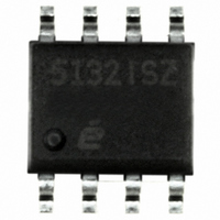
EL5132ISZ-T7 Intersil, EL5132ISZ-T7 Datasheet - Page 11

EL5132ISZ-T7
Manufacturer Part Number
EL5132ISZ-T7
Description
IC VFA 670MHZ ULT LO VOLT 8SOIC
Manufacturer
Intersil
Datasheet
1.EL5132IS.pdf
(13 pages)
Specifications of EL5132ISZ-T7
Amplifier Type
Voltage Feedback
Number Of Circuits
1
Slew Rate
1000 V/µs
Gain Bandwidth Product
3GHz
-3db Bandwidth
670MHz
Current - Input Bias
12µA
Voltage - Input Offset
500µV
Current - Supply
11mA
Current - Output / Channel
140mA
Voltage - Supply, Single/dual (±)
5 V ~ 12 V, ±2.5 V ~ 6 V
Operating Temperature
-40°C ~ 85°C
Mounting Type
Surface Mount
Package / Case
8-SOIC (3.9mm Width)
Lead Free Status / RoHS Status
Lead free / RoHS Compliant
Output Type
-
Other names
EL5132ISZ-T7TR
less, and disabled when CE is above 4V. Although the logic
levels are not standard TTL, this choice of logic voltages
allows the EL5132 to be enabled by typing CE to ground,
even in 5V single supply applications. The CE pin can be
driving from CMOS outputs.
Supply Voltage Range and Single-Supply
Operation
The EL5132 and EL5133 have been designed to operate
with supply voltages having a span of greater than 5V and
less than 12V. In practical terms, this means that they will
operate on dual supplies ranging from ±2.5V to ±6V. With
single-supply, the EL5132 and EL5133 will operate from 5V
to 12V. To prevent internal circuit latch-up, the slew rate
between the negative and positve supplies must be less
than 1V/µs.
As supply voltages continue to decrease, it becomes
necessary to provide input and output voltage ranges that
can get as close as possible to the supply voltages. The
EL5132 and EL5133 have an input range which extends to
within 2V of either supply. So, for example, on ±5V supplies,
the EL5132 and EL5133 have an input range which spans
±3V. The output range of the EL5132 and EL5133 are also
quite large, extending to within 2V of the supply rail. On a
±5V supply, the output is therefore capable of swinging from
-3.1V to +3.1V. Single-supply output range is larger because
of the increased negative swing due to the external pull-
down resistor to ground.
Power Dissipation
With the wide power supply range and large output drive
capability of the EL5132 and EL5133, it is possible to exceed
the 150°C maximum junction temperatures under certain
load and power-supply conditions. It is therefore important to
calculate the maximum junction temperature (T
applications to determine if power supply voltages, load
conditions, or package type need to be modified for the
EL5132 and EL5133 to remain in the safe operating area.
These parameters are related as follows:
where:
• P
• PD
T
PD
JMAX
dissipation of each amplifier in the package (PD
MAX
DMAXTOTAL
MAX
=
=
T
for each amplifier can be calculated as follows:
2*V
MAX
S
+
×
is the sum of the maximum power
(
I
θ
SMAX
JA
xPD
+
MAXTOTAL
(
V
S
11
- V
OUTMAX
)
)
×
V
--------------------------- -
OUTMAX
JMAX
R
L
MAX
) for all
EL5132, EL5133
(EQ. 2)
(EQ. 1)
)
where:
• T
• θ
• PD
• V
• I
• V
• R
Power Supply Bypassing And Printed Circuit
Board Layout
As with any high frequency devices, good printed circuit
board layout is essential for optimum performance. Ground
plane construction is highly recommended. Pin lengths
should be kept as short as possible. The power supply pins
must be closely bypassed to reduce the risk of oscillation.
The combination of a 4.7µF tantalum capacitor in parallel
with 0.1µF ceramic capacitor has been proven to work well
when placed at each supply pin. For single supply operation,
where pin 4 (V
4.7µF tantalum capacitor in parallel with a 0.1µF ceramic
capacitor across pin 8 (V
For good AC performance, parasitic capacitance should be
kept to a minimum. Ground plane construction again should
be used. Small chip resistors are recommended to minimize
series inductance. Use of sockets should be avoided since
they add parasitic inductance and capacitance which will
result in additional peaking and overshoot.
application
MAX
JA
MAX
S
OUTMAX
L
MAX
= Load resistance
= Supply voltage
= Thermal resistance of the package
= Maximum supply current of 1 amplifier
= Maximum ambient temperature
= Maximum power dissipation of 1 amplifier
= Maximum output voltage swing of the
S
-) is connected to the ground plane, a single
S
+).
May 4, 2007
FN7382.8


