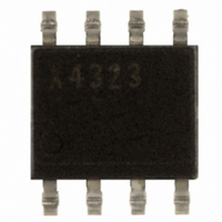
X4323S8I Intersil, X4323S8I Datasheet

X4323S8I
Specifications of X4323S8I
Available stocks
Related parts for X4323S8I
X4323S8I Summary of contents
Page 1
... CC falls below the set minimum thresholds are available, however, Inter- TRIP RESET (X4323) RESET (X4325) Reset & Timebase Reset | Intersil (and design registered trademark of Intersil Americas Inc. Copyright Intersil Americas Inc. 2005-2006. All Rights Reserved trip CC returns to ...
Page 2
PIN CONFIGURATION 8-Pin JEDEC SOIC RST/RST 8-Pin TSSOP PIN FUNCTION Pin ...
Page 3
... X4323V8I-2.7A 4323 AP X4325V8I-2.7A X4323V8IZ-2.7A 4323 APZ X4325V8IZ-2.7A (Note) (Note) X4323S8 X4323 X4325S8 X4323S8Z X4323 Z X4325S8Z (Note) (Note) X4323S8I X4323 I X4325S8I X4323S8IZ X4323 ZI X4325S8IZ (Note) (Note) X4323V8 4323 X4325V8 X4323V8Z 4323 Z X4325V8Z (Note) (Note) X4323V8I 4323 I X4325V8I X4323V8IZ 4323 IZ X4325V8IZ (Note) (Note) X4323S8-4 ...
Page 4
... NOTE: Intersil Pb-free plus anneal products employ special Pb-free material sets; molding compounds/die attach materials and 100% matte tin plate termination finish, which are RoHS compliant and compatible with both SnPb and Pb-free soldering operations. Intersil Pb-free products are MSL classified at Pb-free peak reflow temperatures that meet or exceed the Pb-free requirements of IPC/JEDEC J STD-020. ...
Page 5
PRINCIPLES OF OPERATION Power-on Reset Application of power to the X4323, X4325 activates a Power-on Reset Circuit that pulls the RESET/RESET pin active. This signal provides several benefits. – It prevents the system microprocessor from starting to operate with insufficient ...
Page 6
Setting the V Voltage TRIP This procedure is used to set the V lower voltage value necessary to reset the trip point before setting the new value. To set the new V voltage, start by setting the WEL ...
Page 7
Figure 4. V Programming Sequence TRIP New V Applied = CC Old V Applied + Error CC Emax = Maximum Allowed V Control Register The Control Register provides the user a mechanism for changing the Block Lock and Watchdog Timer ...
Page 8
The state of the Control Register can be read at any time by performing a random read at address FFFFh. Only one byte is read by each register read operation. The X4323, X4325 resets itself after the first byte is ...
Page 9
Writing to the Control Register Changing any of the nonvolatile bits of the control reg- ister requires the following steps: – Write a 02H to the Control Register to set the Write Enable Latch (WEL). This is a volatile operation, ...
Page 10
Serial Start Condition All commands are preceded by the start condition, which is a HIGH to LOW transition of SDA when SCL is HIGH. The device continuously monitors the SDA and SCL lines for the start condition and will not ...
Page 11
Serial Write Operations B W YTE RITE For a write operation, the device requires the Slave Address Byte and a Word Address Byte. This gives the master access to any one of the words in the array. After receipt of ...
Page 12
Figure 10. Writing 12-bytes to a 64-byte Page Starting at Location 60. 8 Bytes Address = 7 The master terminates the Data Byte loading by issuing a stop condition, which causes the device to begin the nonvolatile write cycle. As ...
Page 13
Serial Read Operations Read operations are initiated in the same manner as write operations with the exception that the R/W bit of the Slave Address Byte is set to one. There are three basic read operations: Current Address Reads, Ran- ...
Page 14
There is a similar operation, called “Set Current Address” where the device does no operation, but enters a new address into the address counter if a stop is issued instead of the second start shown in Fig- ure 13. The ...
Page 15
Figure 15. X4323, X4325 Addressing Device Identifier (X1) (X0 Operational Notes The device powers-up in the following state: – The device is in the low power standby state. – The WEL bit is set to ...
Page 16
ABSOLUTE MAXIMUM RATINGS Temperature under bias ................... -65°C to +135°C Storage temperature ........................ -65°C to +150°C Voltage on any pin with respect to V D.C. output current ............................................... 5mA Lead temperature (soldering, 10s) .................... 300°C . RECOMMENDED OPERATING CONDITIONS Temperature ...
Page 17
CAPACITANCE (T = 25° 1.0 MHz Symbol (4) C Output Capacitance (SDA, RST/RST) OUT (4) C Input Capacitance (SCL, WP) IN Notes: (4) This parameter is periodically sampled and not 100% tested. EQUIVALENT A.C. LOAD CIRCUIT ...
Page 18
TIMING DIAGRAMS Bus Timing t F SCL t SU:STA t HD:STA SDA IN SDA OUT WP Pin Timing SCL SDA IN WP Write Cycle Timing SCL 8th bit of Last Byte SDA Nonvolatile Write Cycle Timing Symbol (1) t Write ...
Page 19
Power-Up and Power-Down Timing V TRIP Volts t R RESET (X4323) RESET (X4325) RESET Output Timing Symbol V Reset Trip Point Voltage, X4323-4.5A, X4325-4.5A TRIP Reset Trip Point Voltage, X4323, X4325 Reset Trip Point Voltage, X4323-2.7A, X4325-2.7A ...
Page 20
RESET Output Timing Symbol Parameter t Watchdog Time Out Period, WDO WD1 = 1, WD0 = 1 (factory setting) WD1 = 1, WD0 = 0 WD1 = 0, WD0 = 1 WD1 = 0, WD0 = 0 t Reset Time ...
Page 21
Small Outline Package Family (SO PIN #1 I.D. MARK 0.010 SEATING PLANE 0.004 C 0.010 MDP0027 SMALL OUTLINE PACKAGE FAMILY (SO) SYMBOL SO-8 SO-14 ...
Page 22
... Accordingly, the reader is cautioned to verify that data sheets are current before placing orders. Information furnished by Intersil is believed to be accurate and reliable. However, no responsibility is assumed by Intersil or its subsidiaries for its use; nor for any infringements of patents or other rights of third parties which may result from its use ...


