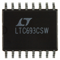
LTC693CSW Linear Technology, LTC693CSW Datasheet - Page 12

LTC693CSW
Manufacturer Part Number
LTC693CSW
Description
IC MPU SUPERVISRY CIRCUIT 16SOIC
Manufacturer
Linear Technology
Type
Simple Reset/Power-On Resetr
Datasheet
1.LTC692CS8PBF.pdf
(20 pages)
Specifications of LTC693CSW
Number Of Voltages Monitored
1
Output
Open Drain or Open Collector
Reset
Active High/Active Low
Reset Timeout
140 ms Minimum
Voltage - Threshold
4.4V
Operating Temperature
0°C ~ 70°C
Mounting Type
Surface Mount
Package / Case
16-SOIC (0.300", 7.5mm Width)
Lead Free Status / RoHS Status
Contains lead / RoHS non-compliant
Other names
LTC693CS
Available stocks
Company
Part Number
Manufacturer
Quantity
Price
Part Number:
LTC693CSW
Manufacturer:
LINEAR/凌特
Quantity:
20 000
Part Number:
LTC693CSW#TRPBF
Manufacturer:
LTNEAR
Quantity:
20 000
LTC692/LTC693
Power-Fail Warning
The LTC692/LTC693 generate a power failure output
(PFO) for early warning of failure in the microprocessor’s
power supply. This is accomplished by comparing the
power failure input (PFI) with an internal 1.3V reference.
PFO goes low when the voltage at the PFI pin is less than
1.3V. Typically PFI is driven by an external voltage divider
(R1 and R2 in Figures 8 and 9) which senses either an
unregulated DC input or a regulated 5V output. The volt-
age divider ratio can be chosen such that the voltage at
the PFI pin falls below 1.3V, several milliseconds before
the 5V supply falls below the maximum reset voltage
threshold of 4.50V. PFO is normally used to interrupt the
microprocessor to execute shutdown procedure between
PFO and RESET or RESET.
APPLICATIONS INFORMATION
12
5V
5V
0.1μF
0.1μF
Figure 6. A Typical Nonvolatile CMOS RAM Application
3V
3V
Figure 7. Write-Protect for RAM with the LTC692
V
V
V
V
BATT
CC
GND
CC
BATT
LTC693
LTC692
GND
CE OUT
RESET
RESET
RESET
CE IN
V
V
OUT
OUT
TO μP
FROM DECODER
+
+
20ns PROPAGATION DELAY
The power-fail comparator, C3, does not have hysteresis.
Hysteresis can be added however, by connecting a resistor
between the PFO output and the noninverting PFI input
pin as shown in Figures 8 and 9. The upper and lower trip
points in the comparator are established as follows:
When PFO output is low, R3 sinks current from the sum-
ming junction at the PFI pin.
When PFO output is high, the series combination of R3
and R4 source current into the PFI summing junction.
10μF
10μF
V = 1.3V 1+
V
As s suming R4
H
L
=
1.3V 1
0.1μF
0.1μF
CS
⎛
⎝ ⎜
⎛
⎝ ⎜
+
CS
V
CS1
CS2
V
<<
R2
R1
CC
R2
CC
R1
62512
RAM
GND
GND
62128
692_3 • F06
RAM
692_3 • F07
+
R3,V
–
R3
R1
1.3V(R3 R4)
(5V – 1.3V)R1
HYSTERESIS
⎞
⎠ ⎟
+
=
⎞
⎠ ⎟
5V
R3
R1
0692fb


