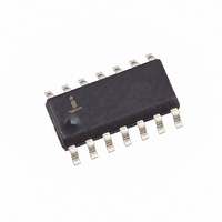
X40431S14I-B Intersil, X40431S14I-B Datasheet - Page 19

X40431S14I-B
Manufacturer Part Number
X40431S14I-B
Description
IC VOLT MON TRPL EEPROM 14-SOIC
Manufacturer
Intersil
Type
Multi-Voltage Supervisorr
Datasheet
1.X40430S14Z-A.pdf
(26 pages)
Specifications of X40431S14I-B
Number Of Voltages Monitored
3
Output
Open Drain or Open Collector
Reset
Active Low
Reset Timeout
Adjustable/Selectable
Voltage - Threshold
1.7V, 2.6V, 4.4V
Operating Temperature
-40°C ~ 85°C
Mounting Type
Surface Mount
Package / Case
14-SOIC (3.9mm Width), 14-SOL
Lead Free Status / RoHS Status
Contains lead / RoHS non-compliant
Available stocks
Company
Part Number
Manufacturer
Quantity
Price
Company:
Part Number:
X40431S14I-B
Manufacturer:
Intersil
Quantity:
100
D.C. OPERATING CHARACTERISTICS
(Over the recommended operating conditions unless otherwise specified)
Notes: (1) The device enters the Active state after any start, and remains active until: 9 clock cycles later if the Device Select Bits in the Slave
EQUIVALENT INPUT CIRCUIT FOR VxMON (x = 1, 2, 3)
CAPACITANCE
Note:
V
Second Supply Monitor
Third Supply Monitor
V
V
V
Symbol
t
t
RPD2
RPD3
CC
Symbol
TRIP1
TRIP2
TRIP3
C
C
I
I
OUT
V2
V3
∆V
IN
Supply
(2) The device goes into Standby: 200ns after any stop, except those that initiate a high voltage write cycle; t
(3) V
(4) At 25°C, V
(5) See ordering information for standard programming levels. For custom programmed levels, contact factory.
(6) Based on characterization data.
(6)
(6)
(1)
(1) This parameter is not 100% tested.
(5)
(5)
(5)
(1)
Address Byte are incorrect; 200ns after a stop ending a read operation; or t
voltage cycle; or 9 clock cycles after any start that is not followed by the correct Device Select Bits in the Slave Address Byte.
IL
V
V2MON Current
V2MON Trip Point Voltage Range
V
V3MON Current
V3MON Trip Point Voltage Range
V
Min. and V
TRIP2
TRIP3
CC
Output Capacitance (SDA, RESET/RESET, LOWLINE,
V2FAIL,V3FAIL, WDO)
Input Capacitance (SCL, WP, MR)
V
Trip Point Voltage Range
ref
CC
to V2FAIL
to V3FAIL
= 3V
IH
Max. are for reference only and are not tested.
Parameter
19
VxMON
Parameter
X40430, X40431, X40434, X40435
R
(Continued)
C
V
REF
4.55
4.35
2.85
2.85
2.55
2.15
1.25
0.95
1.65
3.05
2.85
Min
2.0
1.7
0.9
1.7
+
–
Typ
4.6
4.4
2.9
2.9
2.6
2.2
1.3
1.0
1.7
3.1
2.9
t
RPDX
(4)
= 5µs worst case
WC
Output Pin
Max
4.75
4.65
4.45
2.95
4.75
2.95
2.65
2.25
1.35
1.05
4.75
1.75
3.15
2.95
after a stop ending a write operation.
3.5
15
15
5
5
Max
8
6
Unit
µA
µA
µs
µs
V
V
V
V
V
V
V
V
V
V
V
V
V
V
V
X40430, X40431-A, X40434,
X40435
X40430, X40431-B
X40430, X40431-C
x40430, X40431
x40434, X40435
X40430, X40431-A
X40430, X40431-B
X40430, X40431-C
X40434, X40435-A&B
X40434, X40435-C
X40430, X40431
X40434, X40435-A
X40434, X40435-B&C
Unit
pF
pF
WC
Test Conditions
after a stop that initiates a high
∆V = 100mV
Test Conditions
V
V
OUT
IN
= 0V
= 0V
May 24, 2006
FN8251.1


