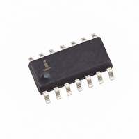
X40431S14I-B Intersil, X40431S14I-B Datasheet - Page 9

X40431S14I-B
Manufacturer Part Number
X40431S14I-B
Description
IC VOLT MON TRPL EEPROM 14-SOIC
Manufacturer
Intersil
Type
Multi-Voltage Supervisorr
Datasheet
1.X40430S14Z-A.pdf
(26 pages)
Specifications of X40431S14I-B
Number Of Voltages Monitored
3
Output
Open Drain or Open Collector
Reset
Active Low
Reset Timeout
Adjustable/Selectable
Voltage - Threshold
1.7V, 2.6V, 4.4V
Operating Temperature
-40°C ~ 85°C
Mounting Type
Surface Mount
Package / Case
14-SOIC (3.9mm Width), 14-SOL
Lead Free Status / RoHS Status
Contains lead / RoHS non-compliant
Available stocks
Company
Part Number
Manufacturer
Quantity
Price
Company:
Part Number:
X40431S14I-B
Manufacturer:
Intersil
Quantity:
100
Setting a V
There are two procedures used to set the threshold
voltages (V
to be stored is higher or lower than the present value.
For example, if the present V
new V
directly into the V
is to be lower than the present setting, then it is neces-
sary to “reset” the V
new value.
Setting a Higher V
To set a V
higher than the present threshold, the user must apply
the desired V
sponding input pin Vcc(V1MON), V2MON or V3MON.
Then, a programming voltage (Vp) must be applied to the
WDO pin before a START condition is set up on SDA.
Next, issue on the SDA pin the Slave Address A0h, fol-
lowed by the Byte Address 01h for V
V
to program V
operation initiates the programming sequence. Pin WDO
must then be brought LOW to complete the operation. To
check if the V
slightly greater than V
Slowly ramp down VXMON and observe when the corre-
sponding outputs (LOWLINE, V2FAIL and V3FAIL)
switch. The voltage at which this occurs is the V
(actual).
C
Now if the desired V
(actual), then add the difference between V
(desired) – V
desired. This is your new V
applied to VXMON and the whole sequence should be
repeated again (see Figure 5).
C
Now if the V
(desired), perform the reset sequence as described in
the next section. The new V
to VXMON will now be: V
(actual) – V
Note: This operation does not corrupt the memory array.
Setting a Lower V
In order to set V
present value, then V
ing to the procedure described below. Once V
TRIP2
ASE
ASE
, and 0Dh for V
A
B
TRIPx
TRIPX
TRIPx
TRIPx
TRIPx
is 3.2 V, the new voltage can be stored
TRIPx
TRIPX
TRIPX
TRIPX
TRIPx
), depending if the threshold voltage
TRIPx
threshold to a new voltage which is
(desired)).
Voltage (x = 1, 2, 3)
. The STOP bit following a valid write
TRIPx
has been set, set VXMON to a value
TRIPx
(actual), is higher than the V
TRIPx
TRIP3
TRIPX
TRIPx
threshold voltage to the corre-
TRIPx
(actual) to the original V
TRIPX
cell. If however, the new setting
Voltage (x = 1, 2, 3)
to a lower voltage than the
Voltage (x = 1, 2, 3)
, and a 00h Data Byte in order
must first be “reset” accord-
9
is greater than the V
voltage before setting the
TRIPX
TRIPX
(that was previously set).
TRIPx
TRIPX
voltage to be applied
(desired) – (V
is 2.9 V and the
X40430, X40431, X40434, X40435
that should be
TRIP1
, 09h for
TRIPX
TRIPX
TRIPX
TRIPX
TRIPX
TRIPX
TRIPx
has been “reset”, then V
voltage using the procedure described in “Setting a
Higher V
Resetting the V
To reset a V
age (Vp) to the WDO pin before a START condition is
set up on SDA. Next, issue on the SDA pin the Slave
Address A0h followed by the Byte Address 03h for
V
by 00h for the Data Byte in order to reset V
STOP bit following a valid write operation initiates the
programming sequence. Pin WDO must then be
brought LOW to complete the operation.
After being reset, the value of V
nal value of 1.7V or lesser.
Notes: 1. This operation does not corrupt the memory array.
CONTROL REGISTER
The Control Register provides the user a mechanism
for changing the Block Lock and Watchdog Timer set-
tings. The Block Lock and Watchdog Timer bits are
nonvolatile and do not change when power is removed.
The Control Register is accessed with a special pream-
ble in the slave byte (1011) and is located at address
1FFh. It can only be modified by performing a byte write
operation directly to the address of the register and only
one data byte is allowed for each register write opera-
tion. Prior to writing to the Control Register, the WEL
and RWEL bits must be set using a two step process,
with the whole sequence requiring 3 steps. See "Writing
to the Control Registers" on page 11.
The user must issue a stop, after sending this byte to
the register, to initiate the nonvolatile cycle that stores
WD1, WD0, PUP1, PUP0, and BP. The X40430,
X40431, X40434, X40435 will not acknowledge any
data bytes written after the first byte is entered.
The state of the Control Register can be read at any
time by performing a random read at address 1FFh,
using the special preamble. Only one byte is read by
each register read operation. The master should
supply a stop condition to be consistent with the bus
protocol.
RWEL: Register Write Enable Latch (Volatile)
The RWEL bit must be set to “1” prior to a write to the
Control Register.
PUP1 WD1 WD0
TRIP1
7
, 0Bh for V
2. Set V
TRIPx
V
6
TRIP2
TRIPx
Voltage”.
CC
or V
5
TRIPx
≅ 1.5(V2MON or V3MON), when setting
voltage, apply the programming volt-
TRIP2
TRIP3
Voltage
BP
4
, and 0Fh for V
TRIPx
respectively.
can be set to the desired
3
0
TRIPx
RWEL WEL PUP0
becomes a nomi-
2
TRIP3
1
TRIPx
, followed
May 24, 2006
FN8251.1
. The
0


