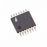
X40626V14I-2.7 Intersil, X40626V14I-2.7 Datasheet - Page 2

X40626V14I-2.7
Manufacturer Part Number
X40626V14I-2.7
Description
IC SUPERVISOR CPU DUAL 14-TSSOP
Manufacturer
Intersil
Type
Multi-Voltage Supervisorr
Datasheet
1.X40626S14.pdf
(22 pages)
Specifications of X40626V14I-2.7
Number Of Voltages Monitored
2
Output
Open Drain or Open Collector
Reset
Active Low
Reset Timeout
100 ms Minimum
Voltage - Threshold
2.63V, 2.63V
Operating Temperature
-40°C ~ 85°C
Mounting Type
Surface Mount
Package / Case
14-TSSOP
Lead Free Status / RoHS Status
Contains lead / RoHS non-compliant
The device’s low V
user’s system from low voltage conditions, resetting the
system when V
point. RESET is asserted until V
operating level and stabilizes. Four industry standard
Vtrip thresholds are available. However, Intersil’s unique
circuits allow the threshold to be reprogrammed to meet
custom requirements or to fine-tune the threshold for
applications requiring higher precision.
The memory portion of the device is a CMOS Serial
EEPROM array with Intersil’s Block Lock
The array is internally organized as 64 bytes per page.
The device features an 2-wire interface and software pro-
tocol allowing operation on an I
PIN FUNCTION
1, 4, 6, 13
Pin
10
11
12
14
2
3
5
7
8
9
CC
V2MON
RESET
V2FAIL
Name
SDA
SCL
V
V
WP
NC
S
S
falls below the set minimum V
CC
SS
0
1
CC
detection circuitry protects the
2
No Internal Connections
Device Select Input
Device Select Input
Reset Output. RESET is an active LOW, open drain output which goes active whenever V
falls below the minimum V
mum V
enabled and SDA remains either HIGH or LOW longer than the selectable Watchdog time-out
period. A falling edge on SDA, while SCL is HIGH, resets the Watchdog Timer. RESET goes
active on power-up and remains active for typically 200ms after the power supply
stabilizes.
Ground
Serial Data. SDA is a bidirectional pin used to transfer data into and out of the device. It has an
open drain output and may be wire ORed with other open drain or open collector outputs. This
pin requires a pull up resistor and the input buffer is always active (not gated).
Watchdog Input. A HIGH to LOW transition on the SDA (while SCL is HIGH) restarts the Watch-
dog timer. The absence of a HIGH to LOW transition within the watchdog time-out
period results in RESET going active.
Serial Clock. The Serial Clock controls the serial bus timing for data input and output.
V2 Voltage Fail Output. This open drain output goes LOW when V2MON is less than V
and goes HIGH when V2MON exceeds V
this pin. This circuit works independently from the Low V
Connect V2FAIL to VSS when not used.
V2 Voltage Monitor Input. When the V2MON input is less than the V
goes LOW. This input can monitor an unregulated power supply with an external resistor
divider or can monitor a second power supply with no external components. Connect V2MON
to V
Write Protect. WP HIGH used in conjunction with WPEN bit prevents writes to the control reg-
ister.
Supply Voltage
2
C bus.
SS
CC
or V
CC
sense level for typically 200ms. RESET goes active if the Watchdog Timer is
returns to proper
CC
when not used. There is no hysteresis in the V2MON comparator circuits.
™
Protection.
CC
trip
CC
X40626
sense level. It will remain active until V
The device utilizes Intersil’s proprietary Direct Write
cell, providing a minimum endurance of 100,000 page
write cycles and a minimum data retention of 100 years.
PIN CONFIGURATION
Function
TRIP2
. There is no power-up reset delay circuitry on
RESET
V
NC
NC
NC
SS
S
S
0
1
CC
14 Pin SOIC/TSSOP
1
2
3
4
5
6
7
reset and battery switch circuits.
CC
TRIP2
14
13
12
11
10
rises above the mini-
9
8
voltage, V2FAIL
V
NC
WP
V2MON
V2FAIL
SCL
SDA
CC
March 28, 2005
TRIP2
FN8119.0
CC
™


