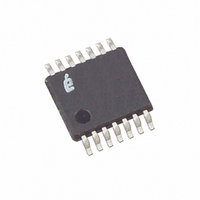
X40626V14I-2.7 Intersil, X40626V14I-2.7 Datasheet

X40626V14I-2.7
Specifications of X40626V14I-2.7
Related parts for X40626V14I-2.7
X40626V14I-2.7 Summary of contents
Page 1
... Generation - V TRIP CAUTION: These devices are sensitive to electrostatic discharge; follow proper IC Handling Procedures. | 1-888-INTERSIL or 1-888-352-6832 Intersil (and design registered trademark of Intersil Americas Inc. All other trademarks mentioned are the property of their respective owners. X40626 64K Bit FN8119.0 V2FAIL RESET Reset Copyright Intersil Americas Inc. 2005. All Rights Reserved ...
Page 2
... V CC point. RESET is asserted until V operating level and stabilizes. Four industry standard Vtrip thresholds are available. However, Intersil’s unique circuits allow the threshold to be reprogrammed to meet custom requirements or to fine-tune the threshold for applications requiring higher precision. ...
Page 3
PRINCIPLES OF OPERATION Power-on Reset Application of power to the X40626 activates a power- on Reset Circuit that pulls the RESET pin active. This signal provides several benefits. – It prevents the system microprocessor from starting to operate with insufficient ...
Page 4
Resetting the V Voltage TRIP This procedure is used to set the V voltage level. For example, if the current V and the new V must be 4.0V, then the V TRIP be reset. When V is reset, the new ...
Page 5
Figure 4. V Programming Sequence TRIP New V applied = X Old V applied + | Error | X Error < MDE 5 X40626 V Programming TRIPX Desired No V TRIPX Present Value YES Set V = Desired V X ...
Page 6
Control Register The Control Register provides the user a mechanism for changing the Block Lock and Watchdog Timer set- tings. The Block Lock and Watchdog Timer bits are nonvolatile and do not change when power is removed. The Control Register ...
Page 7
Table 1. Write Protect Enable Bit and WP Pin Function Memory Array not WP WPEN Block Protected LOW X Writes OK HIGH 0 Writes OK HIGH 1 Writes OK Writing to the Control Register Changing any of the nonvolatile bits ...
Page 8
Figure 5. Valid Data Changes on the SDA Bus SCL SDA Serial Start Condition All commands are preceded by the start condition, which is a HIGH to LOW transition of SDA when SCL is HIGH. The device continuously monitors the ...
Page 9
Figure 7. Acknowledge Response From Receiver SCL from Master Data Output from Data Output from Receiver Start Serial Write Operations Byte Write For a write operation, the device requires the Slave Address Byte and a Word Address Byte. This gives ...
Page 10
Figure 9. Page Write Operation S T Signals from Slave A the Master Address SDA Bus 1 Signals from the Slave Figure 10. Writing 12 bytes to a 64-byte page ...
Page 11
Figure 11. Acknowledge Polling Sequence Byte load completed by issuing STOP. Enter ACK Polling Issue START Issue Slave Address Byte (Read or Write) NO ACK returned? YES NO Nonvolatile Cycle complete. Continue command sequence? YES Continue Normal Read or Write ...
Page 12
Random Read Random read operation allows the master to access any memory location in the array. Prior to issuing the Slave Address Byte with the R/W bit set to one, the master must first perform a “dummy” write operation. The ...
Page 13
Figure 14. Sequential Read Sequence Signals from Slave the Master Address SDA Bus Signals from the Slave X40626 Addressing Slave Address Byte Following a start condition, the master must output a Slave Address Byte. This ...
Page 14
Figure 15. X40626 Addressing Device Identifier 1 A15 A7 D7 Operational Notes The device powers-up in the following state: – The device is in the low power standby state. – The WEL bit is set to ‘0’. In this state ...
Page 15
ABSOLUTE MAXIMUM RATINGS Temperature under bias ................... -65°C to +135°C Storage temperature ........................ -65°C to +150°C Voltage on any pin with respect to VSS... -1.0V to +7V D.C. output current (sink) ................................... 10mA Lead temperature (soldering, 10 seconds) ........ 300°C ...
Page 16
CAPACITANCE (T = 25° 1.0 MHz Symbol (4) C Output Capacitance (SDA, RESET, V2FAIL) OUT (4) C Input Capacitance (SCL, WP, S0, S1) IN Notes: (4) This parameter is periodically sampled and not 100% tested. EQUIVALENT ...
Page 17
TIMING DIAGRAMS Bus Timing t F SCL t SU:STA t HD:STA SDA IN SDA OUT WP Pin Timing SCL SDA IN WP Write Cycle Timing SCL SDA 8th bit of Last Byte Nonvolatile Write Cycle Timing Symbol (1) t Write ...
Page 18
Power-Up and Power-Down Timing V /V TRIP TRIP2 V /V2MON CC 0 Volts t R RESET/V2FAIL RESET Output Timing Symbol t Power-up Reset Timeout PURST ( Detect to Reset/Output (Falling Edge) RPD CC ( /V2MON Fall ...
Page 19
RESET Output Timing Symbol Parameter t Watchdog Timeout Period, WDO WD1 = 1, WD0 = 1 (factory setting) WD1 = 1, WD0 = 0 WD1 = 0, WD0 = 1 WD1 = 0, WD0 = 0 t Reset Timeout RST ...
Page 20
Packaging Information 14-Lead Plastic Small Outline Gullwing Package Type S Pin 1 Index Pin 1 0.014 (0.35) 0.020 (0.51) (4X) 7° 0.050 (1.27) 0.010 (0.25) 0.020 (0.50) 0° - 8° 0.016 (0.410) 0.037 (0.937) NOTE: ALL DIMENSIONS IN INCHES (IN ...
Page 21
PACKAGING INFORMATION 0° - 8° See Detail “A” NOTE: ALL DIMENSIONS IN INCHES (IN PARENTHESES IN MILLIMETERS) 21 X40626 14-Lead Plastic, TSSOP, Package Code V14 .025 (.65) BSC .169 (4.3) .177 (4.5) .193 (4.9) .200 (5.1) .0075 (.19) .002 (.05) ...
Page 22
... SOIC/TSSOP X40626 SOIC V = TSSOP YYWWXX XX – Part Mark WW – Workweek YY – Year Part Number RESET Park (Active LOW) Mark X40626S14-4.5A AL X40626S14I-4.5A AM X40626V14-4.5A AL X40626V14I-4.5A AM X40626S14 blank X40626S14I I X40626V14 blank X40626V14I I X40626S14-2.7A AN X40626S14I-2.7A AP X40626V14-2.7A BN X40626V14I-2.7A AP X40626S14-2.7 F X40626S14I-2.7 G X40626V14-2.7 F X40626V14I-2.7 G FN8119.0 March 28, 2005 ...


