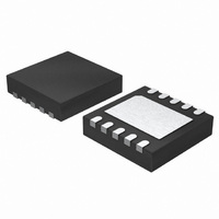
ISL9012IRPLZ Intersil, ISL9012IRPLZ Datasheet

ISL9012IRPLZ
Specifications of ISL9012IRPLZ
Related parts for ISL9012IRPLZ
ISL9012IRPLZ Summary of contents
Page 1
... CAUTION: These devices are sensitive to electrostatic discharge; follow proper IC Handling Procedures. 1-888-INTERSIL or1-888-468-3774 All other trademarks mentioned are the property of their respective owners. ISL9012 March 11, 2008 FN9220.3 @ 100µA (1.5V) RMS | Intersil (and design registered trademark of Intersil Americas Inc. Copyright © Intersil Americas Inc. 2005, 2006. 2008. All Rights Reserved. ...
Page 2
... DAAF ISL9012IRJBZ DAWA ISL9012IRGCZ DAAE ISL9012IRFJZ DAYA ISL9012IRFDZ DCBK ISL9012IRFCZ DCBL ISL9012IRPLZ DAAD ISL9012IRCJZ DCBN ISL9012IRCCZ DCBP ISL9012IRBJZ DAAC NOTES: 1. Please refer to TB347 for details on reel specifications. 2. For other output voltages, contact Intersil Marketing. 3. These Intersil Pb-free plastic packaged products employ special Pb-free material sets; molding compounds/die attach materials and 100% matte tin plate PLUS ANNEAL - e3 termination finish, which is RoHS compliant and compatible with both SnPb and Pb-free soldering operations ...
Page 3
... Thermal Resistance (Notes 4, 5) 3x3 DFN Package . . . . . . . . . . . . . . . . + 0.3)V IN Junction Temperature Range . . . . . . . . . . . . . . . . .-40°C to +125°C Operating Temperature Range . . . . . . . . . . . . . . . . .-40°C to +85°C Storage Temperature Range . . . . . . . . . . . . . . . . . .-65°C to +150°C Pb-free Reflow Profile . . . . . . . . . . . . . . . . . . . . . . . . .see link below http://www.intersil.com/pbfree/Pb-FreeReflow.asp = (V + 0.5V) to 6.5V with a minimum 0.01µ 0.01µF POR ...
Page 4
Electrical Specifications Unless otherwise noted, all parameters are guaranteed over the operational supply voltage and temperature range of the device as follows -40°C to +85° BYP PARAMETER SYMBOL Output Noise Voltage DEVICE START-UP CHARACTERISTICS Device ...
Page 5
Typical Performance Curves 0.8 0.6 0.4 0.2 -40°C 0.0 +25°C -0.2 +85°C -0.4 -0.6 -0.8 3.4 3.8 4.2 4.6 5.0 INPUT VOLTAGE (V) FIGURE 2. OUTPUT VOLTAGE vs INPUT VOLTAGE (3.3V OUTPUT) 0.10 0.08 0.06 0.04 0.02 0.00 -0.02 -0.04 ...
Page 6
Typical Performance Curves 175 VO1 = 3.3V 150 125 +85°C 100 100 OUTPUT LOAD (mA) FIGURE 8. VO1 DROPOUT VOLTAGE vs LOAD CURRENT 200 180 160 140 +85°C 120 100 80 60 ...
Page 7
Typical Performance Curves VO2 (10mV/DIV 100 200 300 400 500 600 TIME (µs) FIGURE 14. TURN ON/TURN OFF RESPONSE 4.2V 3.5V 10mV/DIV 400µs/DIV FIGURE 16. LINE TRANSIENT RESPONSE, 2.8V OUTPUT 100 90 80 ...
Page 8
Pin Description PIN PIN NUMBER NAME TYPE 1 VIN Analog I/O 2 EN1 Low Voltage Compatible CMOS Input 3 EN2 Low Voltage Compatible CMOS Input 4 CBYP Analog I/O 5 CPOR Analog I/O 6 GND Ground ...
Page 9
Block Diagram IS2 1V QEN2 LDO-2 LDO-1 EN1 EN2 UVLO GND Functional Description The ISL9012 contains all circuitry required to implement two high performance LDO’s. High performance is achieved through a circuit that delivers fast transient response to varying load ...
Page 10
VO2 turn-on until the VO1 output reaches its target level. If EN2 is brought high, and EN1 goes high after VO2 starts its output ramp, then the ISL9012 immediately starts to ramp up the VO1 output. If both ...
Page 11
... Accordingly, the reader is cautioned to verify that data sheets are current before placing orders. Information furnished by Intersil is believed to be accurate and reliable. However, no responsibility is assumed by Intersil or its subsidiaries for its use; nor for any infringements of patents or other rights of third parties which may result from its use ...


