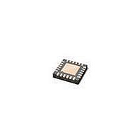
TFF1003HN/N1,115 NXP Semiconductors, TFF1003HN/N1,115 Datasheet - Page 4

TFF1003HN/N1,115
Manufacturer Part Number
TFF1003HN/N1,115
Description
IC FREQUENCY GEN TX/TXRX 24HVQFN
Manufacturer
NXP Semiconductors
Type
Ku Frequency Generatorr
Datasheet
1.TFF1003HNN1118.pdf
(17 pages)
Specifications of TFF1003HN/N1,115
Package / Case
24-VFQFN Exposed Pad
Mounting Type
Surface Mount
Voltage - Supply
3 V ~ 3.6 V
Frequency-max
13.05GHz
Operating Temperature
-40°C ~ 85°C
Output
Clock
Input
Clock
Maximum Input Frequency
816 MHz
Minimum Input Frequency
50 MHz
Output Frequency Range
12.8 GHz to 13.05 GHz
Supply Voltage (max)
3.6 V
Supply Voltage (min)
3 V
Input Level
- 10 dBm
Mounting Style
SMD/SMT
Operating Supply Voltage
3.3 V
Output Level
- 5 dBm
Lead Free Status / RoHS Status
Lead free / RoHS Compliant
NXP Semiconductors
9. Pinning information
TFF1003HN_1
Product data sheet
9.1 Pinning
9.2 Pin description
Table 4.
Symbol
VREGVCO
CPOUT
VTUNE
NSL0
NSL1
NSL2
LCKDET
GND1(REF) 8
IN(REF)_P
IN(REF)_N
GND2(REF) 11
V
V
GND(DIV)
n.c.
n.c.
GND1(BUF) 17
Fig 3.
CC(REF)
CC(DIV)
Pin configuration for HVQFN24
Pin description
Pin Description
1
2
3
4
5
6
7
9
10
12
13
14
15
16
All information provided in this document is subject to legal disclaimers.
Regulated output voltage for VCO loop filter. Connect loop filter to this pin.
Charge pump output.
Tuning voltage for VCO.
Divider setting, LSB. Leave open for “1”, connect to GND for “0”. See
Divider setting. Leave open for “1”, connect to GND for “0”. See
Divider setting, MSB. Leave open for “1”, connect to GND for “0”. See
Lock detect. Lock = 2.5 V; out of lock = 0 V. See
Ground for REF input. Connect this pin to the exposed diepad landing.
Reference signal, non-inverting input. Couple this AC to the source.
Reference signal, inverting input. Couple this AC to the source.
Ground for REF input. Connect this pin to the exposed diepad landing.
Supply of the internal regulated voltages. Decouple this pin against
GND2(REF) (pin 11).
Supply of the divider and PFD/CP. Decouple this pin against GND(DIV)
(pin 14).
Ground of the divider. Connect this pin to the exposed diepad landing.
not connected
not connected
Ground for RF output. Connect this pin to the exposed diepad landing.
Rev. 01 — 19 May 2010
index area
terminal 1
VREGVCO
CPOUT
VTUNE
NSL0
NSL1
NSL2
Low phase noise LO generator for VSAT applications
1
2
3
4
5
6
Transparent top view
18
17
16
15
14
13
001aal726
V
GND1(BUF)
n.c.
n.c.
GND(DIV)
V
CC(BUF)
CC(DIV)
Table
TFF1003HN
6.
© NXP B.V. 2010. All rights reserved.
Table
Table
8.
Table
4 of 17
8.
8.


