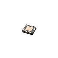
TFF1003HN/N1,115 NXP Semiconductors, TFF1003HN/N1,115 Datasheet - Page 8

TFF1003HN/N1,115
Manufacturer Part Number
TFF1003HN/N1,115
Description
IC FREQUENCY GEN TX/TXRX 24HVQFN
Manufacturer
NXP Semiconductors
Type
Ku Frequency Generatorr
Datasheet
1.TFF1003HNN1118.pdf
(17 pages)
Specifications of TFF1003HN/N1,115
Package / Case
24-VFQFN Exposed Pad
Mounting Type
Surface Mount
Voltage - Supply
3 V ~ 3.6 V
Frequency-max
13.05GHz
Operating Temperature
-40°C ~ 85°C
Output
Clock
Input
Clock
Maximum Input Frequency
816 MHz
Minimum Input Frequency
50 MHz
Output Frequency Range
12.8 GHz to 13.05 GHz
Supply Voltage (max)
3.6 V
Supply Voltage (min)
3 V
Input Level
- 10 dBm
Mounting Style
SMD/SMT
Operating Supply Voltage
3.3 V
Output Level
- 5 dBm
Lead Free Status / RoHS Status
Lead free / RoHS Compliant
NXP Semiconductors
11. Limiting values
TFF1003HN_1
Product data sheet
10.5 Divider settings (NSL2, NSL1, NSL0)
Note that the phase noise of the output signal is also determined by the phase noise of the
reference signal. The reference frequency range is equal to the
output frequency / division value. Note that the output frequency is guaranteed from
12.8 GHz to 13.05 GHz.
The divider can be set to 16, 32, 64, 128 and 256 (See
NSL0 (pin 4), NSL1 (pin 5) and NSL2 (pin 6) are given in
The pins have a pull-up resistor of 100 kΩ to V
The device is only guaranteed when NSL2, NSL1 and NSL0 are predefined at start-up (no
change of divider value is allowed during operation).
Table 7.
The truth table is shown in
Table 8.
[1]
Table 9.
In accordance with the Absolute Maximum Rating System (IEC 60134).
Logical value
0
1
Setting number
0
1
2
3
4
5
6
7
Symbol
V
V
V
T
T
j
stg
CC(REF)
CC(DIV)
CC(BUF)
Test mode, divider output will be disabled.
Logical and physical value for divider setting (NSL2, NSL1, NSL0)
Divider setting as function of NSL2, NSL1 and NSL0
Limiting values
Parameter
reference supply voltage
divider supply voltage
buffer supply voltage
junction temperature
storage temperature
All information provided in this document is subject to legal disclaimers.
NSL2
0
0
0
0
1
1
1
1
Rev. 01 — 19 May 2010
Table
Low phase noise LO generator for VSAT applications
8.
NSL1
0
0
1
1
0
0
1
1
Physical value
GND
open or V
CC(DIV)
Conditions
(pin 13).
CC
NSL0
0
1
0
1
0
1
0
1
Table
Table
8). The logic levels for
7.
TFF1003HN
Min
−0.5
−0.5
−0.5
−40
−40
© NXP B.V. 2010. All rights reserved.
Divider value
16
32
64
128
256
[1]
[1]
[1]
Max
+3.6
+3.6
+3.6
+125
+125
Unit
V
V
V
°C
°C
8 of 17


