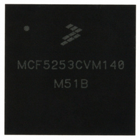
MCF5253CVM140 Freescale Semiconductor, MCF5253CVM140 Datasheet - Page 22

MCF5253CVM140
Manufacturer Part Number
MCF5253CVM140
Description
IC MPU 32BIT 140MHZ 225-MAPBGA
Manufacturer
Freescale Semiconductor
Series
MCF525xr
Datasheets
1.MCF5253VM140J.pdf
(34 pages)
2.MCF5253VM140J.pdf
(8 pages)
3.MCF5253VM140J.pdf
(648 pages)
4.MCF5253VM140J.pdf
(2 pages)
Specifications of MCF5253CVM140
Core Processor
Coldfire V2
Core Size
32-Bit
Speed
140MHz
Connectivity
CAN, EBI/EMI, I²C, QSPI, UART/USART, USB OTG
Peripherals
DMA, WDT
Program Memory Type
ROMless
Ram Size
128K x 8
Voltage - Supply (vcc/vdd)
1.08 V ~ 1.32 V
Data Converters
A/D 6x12b
Oscillator Type
External
Operating Temperature
-40°C ~ 85°C
Package / Case
225-MAPBGA
Family Name
MCF5xxx
Device Core
ColdFire V2
Device Core Size
32b
Frequency (max)
140MHz
Instruction Set Architecture
RISC
Supply Voltage 1 (typ)
1.2/3.3V
Operating Supply Voltage (max)
1.32/3.6V
Operating Supply Voltage (min)
1.08/3V
Operating Temp Range
-40C to 85C
Operating Temperature Classification
Industrial
Mounting
Surface Mount
Pin Count
225
Package Type
MA-BGA
Lead Free Status / RoHS Status
Lead free / RoHS Compliant
Number Of I /o
-
Eeprom Size
-
Program Memory Size
-
Lead Free Status / Rohs Status
Compliant
Available stocks
Company
Part Number
Manufacturer
Quantity
Price
Company:
Part Number:
MCF5253CVM140
Manufacturer:
FREESCALE
Quantity:
300
Company:
Part Number:
MCF5253CVM140
Manufacturer:
Freescale Semiconductor
Quantity:
10 000
Part Number:
MCF5253CVM140
Manufacturer:
FREESCALE
Quantity:
20 000
Company:
Part Number:
MCF5253CVM140J
Manufacturer:
Freescale Semiconductor
Quantity:
10 000
SDATA0_SDIO1/GPIO1
DDATA2/CTS0/GPIO3
DDATA3/RTS0/GPIO4
SDATA2_BS2/GPIO2
XTRIM/TXD2/GPIO0
Package Information and Pinout
22
PSTCLK/GPIO51
PST2/INTMON2/
PST3/INTMON1/
DDATA0/CTS1/
DDATA1/RTS1/
PST0/GPIO50
PST1/GPIO49
TRST/DSCLK
USB_CROUT
ATA_DMARQ
ATA_DMACK
RTCCROUT
ATA_IORDY
ATA_INTRQ
RTC_CRIN
USB_CRIN
ATA_DIOW
TMS/BKPT
ATA_DIOR
TDO/DSO
ATA_CS0
ATA_CS1
ATA_RST
ATA_D15
CROUT
TDI/DSI
GPIO48
GPIO47
TEST0
TEST1
TEST2
Name
CRIN
RSTI
HI_Z
TCK
Drive Type/
Strength
IO / 8 mA
IO / 2 mA
IO / 8 mA
IO / 4 mA
IO / 4 mA
IO / 4 mA
IO / 4 mA
IO / 4 mA
IO / 4 mA
IO / 4 mA
IO / 4 mA
O / 2 mA
O / 2 mA
O / 8 mA
O / 8 mA
O / 8 mA
O / 2 mA
O / 4 mA
A
A
A
A
–
–
I
I
I
I
I
I
I
I
I
I
I
I
MCF5253 ColdFire Processor Data Sheet: Technical Data, Rev. 4
Table 19. 225 MAPBGA Pin Assignment (continued)
Load
(pF)
40
40
40
40
40
40
40
30
30
30
30
30
30
30
30
30
30
30
–
–
–
–
–
–
–
–
–
–
–
–
–
–
–
–
–
–
Function
PSTCLK
DDATA0
DDATA1
DDATA2
DDATA3
XTRIM
PST0
PST1
PST2
PST3
1st
–
–
–
–
–
–
–
–
–
–
–
–
–
–
–
–
–
–
–
–
–
–
–
–
–
–
Clock Generation
CTS1/SDATA
RTS1/SDATA
JTAG/BDM/Test
Function
INTMON2
INTMON1
Reset/Wake-up
0_SDIO1
2_BS2
TXD2
CTS0
RTS0
2nd
–
–
–
–
–
–
–
–
–
–
–
–
–
–
–
–
–
–
–
–
–
–
–
–
–
–
–
–
–
Pinconfig
Register
14,13
24,23
Bit
17
18
22
21
–
–
–
–
–
–
–
–
–
–
–
–
–
–
–
–
0
–
–
–
–
–
–
–
–
–
–
–
–
–
IO51
IO50
IO49
IO48
IO47
Pin
GP
IO0
IO1
IO2
IO3
IO4
–
–
–
–
–
–
–
–
–
–
–
–
–
–
–
–
–
–
–
–
–
–
–
–
–
–
Reset
HI_Z
HI_Z
HI_Z
HI_Z
HI_Z
HI_Z
HI_Z
HI_Z
–
–
–
–
–
–
–
–
–
–
–
–
–
–
–
–
–
–
–
–
–
–
–
–
–
–
–
–
D
C
D
B
A
D
D
A
C
C
M
N
K
R
G
B
G
G
G
H
H
K
R
G
H
E
1
2
9
9
1
5
1
3
7
8
7
1
2
8
3
2
J
1
2
L
1
4
L
1
5
6
1
3
F
1
5
F
1
2
F
1
3
F
1
4
1
3
1
4
1
5
1
2
1
4
1
3
1
0
1
1
J
1
4
J
1
2
F
1
1
1
0
1
0
1
5
Main Processor Clock Input
Main Processor Clock Output
Real Time Clock (32.768 kHz)
Input
Real Time Clock (32.768 kHz)
Output
USB Clock (24 MHz) Input
USB Clock (24 MHz) Output
Interrupt Capable Input
See TEST0 Description
See TEST0 Description
See TEST0 Description
See TEST0 Description
For Normal Operation Tie This Pin
High
Interrupt Capable Input
Interrupt Capable Input
Interrupt Capable Input
Interrupt Capable Input
BDM/JTAG Select: 1-BDM; 0-JTAG
For normal operation, tie this pin
low.
For normal operation, tie this pin
low.
Freescale Semiconductor
Notes
–
–
–
–
–
–
–
–
–
–
–
–
–
–
–
–
–


