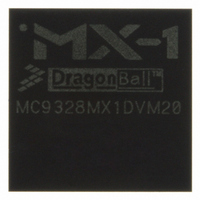
MC9328MX1DVM20 Freescale Semiconductor, MC9328MX1DVM20 Datasheet - Page 90

MC9328MX1DVM20
Manufacturer Part Number
MC9328MX1DVM20
Description
IC MCU I.MX 200MHZ 256-MAPBGA
Manufacturer
Freescale Semiconductor
Series
i.MX1r
Datasheet
1.MC9328MX1DVH20.pdf
(100 pages)
Specifications of MC9328MX1DVM20
Core Processor
ARM9
Core Size
32-Bit
Speed
200MHz
Connectivity
EBI/EMI, I²C, MMC, SmartCard, SPI, SSI, UART/USART, USB
Peripherals
DMA, I²S, LCD, POR, PWM, WDT
Number Of I /o
110
Program Memory Type
ROMless
Voltage - Supply (vcc/vdd)
1.7 V ~ 3.3 V
Oscillator Type
External
Operating Temperature
-30°C ~ 70°C
Package / Case
256-MAPBGA
Lead Free Status / RoHS Status
Lead free / RoHS Compliant
Eeprom Size
-
Ram Size
-
Program Memory Size
-
Data Converters
-
Available stocks
Company
Part Number
Manufacturer
Quantity
Price
Company:
Part Number:
MC9328MX1DVM20
Manufacturer:
Freescale Semiconductor
Quantity:
10 000
Company:
Part Number:
MC9328MX1DVM20R2
Manufacturer:
Freescale Semiconductor
Quantity:
10 000
1
2
3
Functional Description and Application Information
90
Ref
No.
28
29
30
31
32
33
34
All the timings for the SSI are given for a non-inverted serial clock polarity (TSCKP/RSCKP = 0) and a non-inverted frame sync
(TFSI/RFSI = 0). If the polarity of the clock and/or the frame sync have been inverted, all the timing remains valid by inverting
the clock signal STCK/SRCK and/or the frame sync STFS/SRFS shown in the tables and in the figures.
There are 2 set of I/O signals for the SSI module. They are from Port C primary function (pad 257 to pad 261) and Port B
alternate function (pad 283 to pad 288). When SSI signals are configured as outputs, they can be viewed both at Port C primary
function and Port B alternate function. When SSI signals are configured as inputs, the SSI module selects the input based on
FMCR register bits in the Clock controller module (CRM). By default, the input are selected from Port C primary function.
11a
Ref
No.
10
bl = bit length; wl = word length.
1
2
3
4
5
6
7
8
9
STCK high to STXD high impedance
SRXD setup time before SRCK low
SRXD hold time after SRCK low
SRXD setup before STCK falling
SRXD hold after STCK falling
SRXD setup before STCK falling
SRXD hold after STCK falling
STCK/SRCK clock period
STCK high to STFS (bl) high
SRCK high to SRFS (bl) high
STCK high to STFS (bl) low
SRCK high to SRFS (bl) low
STCK high to STFS (wl) high
SRCK high to SRFS (wl) high
STCK high to STFS (wl) low
SRCK high to SRFS (wl) low
STCK high to STXD valid from high impedance
STCK high to STXD high
Table 40. SSI (Port B Alternate Function) Timing Parameter Table (Continued)
Table 41. SSI 2 (Port C Alternate Function) Timing Parameter Table
Synchronous External Clock Operation (Port B Alternate Function
Parameter
Synchronous Internal Clock Operation (Port B Alternate Function
Parameter
Internal Clock Operation
1
3
3
3
3
3
3
3
3
MC9328MX1 Technical Data, Rev. 7
Minimum
1
Minimum
(Port C Alternate Function)
14.93
3.08
1.25
1.71
3.08
1.25
1.25
-0.1
-0.1
17.90
18.81
1.7
95
1.14
1.14
1.8V +/- 0.10V
0
0
0
1.8 ± 0.1 V
Maximum
Maximum
16.19
5.24
2.28
4.79
5.24
2.28
3.42
29.75
4.8
1.0
1.0
–
–
–
–
–
–
–
Minimum
2
Minimum
83.3
13.1
-0.1
-0.1
15.7
16.5
1.5
2.7
1.1
1.5
2.7
1.1
1.1
1.0
1.0
0
0
0
3.0V +/- 0.30V
2
2
3.0 ± 0.3 V
)
)
Freescale Semiconductor
Maximum
Maximum
14.2
26.1
4.2
1.0
4.6
2.0
4.2
1.0
4.6
2.0
3.0
–
–
–
–
–
–
–
Unit
Unit
ns
ns
ns
ns
ns
ns
ns
ns
ns
ns
ns
ns
ns
ns
ns
ns
ns
ns


