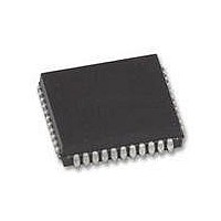
XR68C681J-F Exar Corporation, XR68C681J-F Datasheet - Page 10

XR68C681J-F
Manufacturer Part Number
XR68C681J-F
Description
IC UART CMOS DUAL 44PLCC
Manufacturer
Exar Corporation
Type
CMOS Dual Channel UARTr
Datasheet
1.XR68C681J-F.pdf
(75 pages)
Specifications of XR68C681J-F
Number Of Channels
2, DUART
Package / Case
44-LCC (J-Lead)
Features
*
Fifo's
1 Byte, 3 Byte
Voltage - Supply
5V
Mounting Type
Surface Mount
Data Rate
1 Mbps
Supply Voltage (max)
5.5 V
Supply Voltage (min)
4.5 V
Supply Current
15 mA
Maximum Operating Temperature
+ 85 C
Minimum Operating Temperature
- 40 C
Mounting Style
SMD/SMT
Operating Supply Voltage
5 V
Propagation Delay Time Ns
400 ns
No. Of Channels
2
Supply Voltage Range
4.75V To 5.25V
Operating Temperature Range
-40°C To +85°C
Digital Ic Case Style
PLCC
No. Of Pins
44
Filter Terminals
SMD
Rohs Compliant
Yes
Lead Free Status / RoHS Status
Lead free / RoHS Compliant
Lead Free Status / RoHS Status
Lead free / RoHS Compliant, Lead free / RoHS Compliant
Other names
1016-1324-5
Available stocks
Company
Part Number
Manufacturer
Quantity
Price
Company:
Part Number:
XR68C681J-F
Manufacturer:
Exar Corporation
Quantity:
10 000
AC ELECTRICAL CHARACTERISTICS
Test Conditions: T
Notes
1.
2.
3.
4.
5.
6.
7.
8.
ABSOLUTE MAXIMUM RATINGS
1.
2.
Clock Timing (Figure 38)
Transmitter Timing (Figure 39)
Receiver Timing (Figure 40)
Parameters are valid over the specified temperature and operating supply ranges. Typical values are 25C, V
processing parameters.
All voltages are referenced to ground (GND). For testing, input signal levels are 0.4V and 2.4V with a transition time of 20ns
maximum. All time measurements are referenced at input voltages of 0.8V and 2.0V as appropriate. See Figure 31.
AC test conditions for outputs: CL = 50pF, RL = 2.7k• to V
Consecutive write operations to the same register require at least three edges of the X1 clock between writes.
This specification imposes a 6 MHz maximum 68000 clock frequency if a read or write cycle follows immediately after the previous
read or write cycle. A higher 68000 clock can be used if this is not the case.
This specification imposes a lower bound on CS and IACK low, guaranteeing that they will be low for at least one CLK period.
This parameter is specified only to insure DTACK is asserted with respect to the rising edge of X1/CLK as shown in the timing dia-
gram, not to guarantee operation of the part. If the specified setup time is violated, DTACK may be asserted as shown or may be
asserted one clock cycle later.
The minimum high time must be at least 1.5 times the X1/CLK period and the minimum low time must be at least equal to the X1/CLK
period if either channel’s Receiver is operating in external 1X clock mode.
Stresses above those listed under the Absolute Maximum Ratings may cause permanent damage to the device. This is a stress rat-
ing only, and functional operation of the device at these or any other conditions above those indicated in the “Electrical Characteris-
tics” section of this specification is not implied. Exposure to absolute maximum rating conditions for extended periods may affect
device reliability.
This product includes circuitry specifically designed for the protection of its internal devices from damaging effects of excessive stat-
ic charge. Nonetheless, it is suggested that conventional precautions be taken to avoid applying any voltage larger than the rated
maximum.
XR68C681
Symbol
Parameter
A
= 0 - 70C, V
1
CC
Specifications are subject to change without notice
= 5.0V +5% unless otherwise specified.
1, 2, 3
(CONT’D)
Min
CC
.
Typ
Max
Unit
Conditions
CC
= 5V and typical


