STEVAL-PCC012V1 STMicroelectronics, STEVAL-PCC012V1 Datasheet - Page 57
STEVAL-PCC012V1
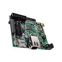
Manufacturer Part Number
STEVAL-PCC012V1
Description
BOARD DEM CONN GATEWAY STM32F107
Manufacturer
STMicroelectronics
Series
STM32r
Type
Other Power Managementr
Datasheets
1.STM32F105V8T6.pdf
(101 pages)
2.STEVAL-PCC012V1.pdf
(10 pages)
3.EVALST7590-1.pdf
(43 pages)
Specifications of STEVAL-PCC012V1
Main Purpose
Interface, Connectivity
Embedded
Yes, MCU, 32-Bit
Utilized Ic / Part
STM32F107
Primary Attributes
Ethernet and 4 Digital/Analog Connectors
Secondary Attributes
On-Board LEDs and Joystick
Interface Type
Ethernet, USB, I2C, SPI, UART
Operating Supply Voltage
3.3 V
Product
Power Management Development Tools
Lead Free Status / RoHS Status
Lead free / RoHS Compliant
For Use With/related Products
STM32F107xx
Other names
497-10757
Available stocks
Company
Part Number
Manufacturer
Quantity
Price
Company:

Part Number:
STEVAL-PCC012V1
Manufacturer:
STMicroelectronics
Quantity:
1


STM32F105xx, STM32F107xx
Output driving current
The GPIOs (general purpose input/outputs) can sink or source up to +/-8 mA, and sink or
source up to +/-20 mA (with a relaxed V
In the user application, the number of I/O pins which can drive current must be limited to
respect the absolute maximum rating specified in
●
●
Output voltage levels
Unless otherwise specified, the parameters given in
performed under ambient temperature and V
Table
Table 36.
1. The I
2. The I
3. Based on characterization data, not tested in production.
V
V
Symbol
V
V
V
V
V
V
OH
OH
OL
OL
OH
OL
OH
and the sum of I
Table 7
OL
(1)(3)
(1)(3)
(2)(3)
(2)(3)
The sum of the currents sourced by all the I/Os on V
consumption of the MCU sourced on V
I
The sum of the currents sunk by all the I/Os on V
consumption of the MCU sunk on V
I
VDD
VSS
(1)
(2)
(1)
(2)
9. All I/Os are CMOS and TTL compliant.
IO
IO
current sunk by the device must always respect the absolute maximum rating specified in
current sourced by the device must always respect the absolute maximum rating specified in
(see
and the sum of I
(see
Output low level voltage for an I/O pin
when 8 pins are sunk at same time
Output high level voltage for an I/O pin
when 8 pins are sourced at same time
Output low level voltage for an I/O pin
when 8 pins are sunk at same time
Output high level voltage for an I/O pin
when 8 pins are sourced at same time
Output low level voltage for an I/O pin
when 8 pins are sunk at same time
Output high level voltage for an I/O pin
when 8 pins are sourced at same time
Output low level voltage for an I/O pin
when 8 pins are sunk at same time
Output high level voltage for an I/O pin
when 8 pins are sourced at same time
Output voltage characteristics
Table
Table
IO
(I/O ports and control pins) must not exceed I
7).
7).
IO
Parameter
(I/O ports and control pins) must not exceed I
Doc ID 15274 Rev 5
OL
SS
/V
DD,
cannot exceed the absolute maximum rating
OH
DD
cannot exceed the absolute maximum rating
).
supply voltage conditions summarized in
2.7 V < V
2.7 V < V
2.7 V < V
2 V < V
Section
I
Conditions
I
IO
I
CMOS port
I
Table 36
IO
IO
IO
TTL port
SS
= +20 mA
= +8 mA
= +6 mA
VSS
=+ 8mA
DD
DD
DD
DD
plus the maximum Run
DD,
.
5.2:
< 2.7 V
< 3.6 V
< 3.6 V
< 3.6 V
plus the maximum Run
VDD
are derived from tests
.
Electrical characteristics
V
V
V
DD
DD
DD
Min
2.4
–0.4
–1.3
–0.4
Max
0.4
0.4
1.3
0.4
Table 7
57/101
Unit
V
V
V
V
Related parts for STEVAL-PCC012V1
Image
Part Number
Description
Manufacturer
Datasheet
Request
R

Part Number:
Description:
Interface Development Tools Opto ISO USB Bridge 8-Pin Motor CTRL BRD
Manufacturer:
STMicroelectronics
Datasheet:

Part Number:
Description:
BOARD EVAL FOR MEMS SENSORS
Manufacturer:
STMicroelectronics
Datasheet:
Part Number:
Description:
EVALBOARD/STEVAL-ISV014V1
Manufacturer:
STMicroelectronics
Part Number:
Description:
BOARD EVAL FOR ST802RT1
Manufacturer:
STMicroelectronics
Datasheet:

Part Number:
Description:
BOARD EVAL FOR VACUUM CLEANER
Manufacturer:
STMicroelectronics
Datasheet:

Part Number:
Description:
KIT DEV STARTER ST10F276Z5
Manufacturer:
STMicroelectronics
Datasheet:

Part Number:
Description:
BOARD LED CTLR/DVR STLED316S
Manufacturer:
STMicroelectronics
Datasheet:

Part Number:
Description:
BOARD EVAL BLDC SENSORLESS MOTOR
Manufacturer:
STMicroelectronics
Datasheet:

Part Number:
Description:
BOARD ELECT FISCAL CASH REGISTER
Manufacturer:
STMicroelectronics
Datasheet:

Part Number:
Description:
BOARD EVAL BIPO SOLUTION FOR PFC
Manufacturer:
STMicroelectronics
Datasheet:
Part Number:
Description:
STMicroelectronics [RIPPLE-CARRY BINARY COUNTER/DIVIDERS]
Manufacturer:
STMicroelectronics
Datasheet:
Part Number:
Description:
STMicroelectronics [LIQUID-CRYSTAL DISPLAY DRIVERS]
Manufacturer:
STMicroelectronics
Datasheet:
Part Number:
Description:
BOARD EVAL FOR MEMS SENSORS
Manufacturer:
STMicroelectronics
Datasheet: