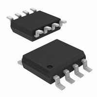
AD8350ARMZ20 Analog Devices Inc, AD8350ARMZ20 Datasheet - Page 11

AD8350ARMZ20
Manufacturer Part Number
AD8350ARMZ20
Description
IC AMP DIFF LOW-DISTORTION 8MSOP
Manufacturer
Analog Devices Inc
Datasheet
1.AD8350ARZ20-REEL7.pdf
(16 pages)
Specifications of AD8350ARMZ20
Current - Supply
28mA
Frequency
0Hz ~ 1GHz
Gain
20dB
Noise Figure
5.9dB
P1db
-2.6dBm
Package / Case
8-TSSOP, 8-MSOP (0.118", 3.00mm Width)
Rf Type
Cellular
Test Frequency
250MHz
Voltage - Supply
5 V ~ 10 V
No. Of Amplifiers
1
Input Offset Voltage
1mV
Gain Db Max
21dB
Bandwidth
0.9GHz
Slew Rate
2000V/µs
Supply Voltage Range
5V To 10V
Supply Current
28mA
Amplifier Case Style
MSOP
No. Of Pins
8
Lead Free Status / RoHS Status
Lead free / RoHS Compliant
Available stocks
Company
Part Number
Manufacturer
Quantity
Price
Part Number:
AD8350ARMZ20
Manufacturer:
ADI/亚德诺
Quantity:
20 000
Part Number:
AD8350ARMZ20-REEL7
Manufacturer:
ADI/亚德诺
Quantity:
20 000
The power gain of any two-port network is dependent on the
source and load impedance. The effective gain will change if the
differential source and load impedance is not 200 Ω. The single-
ended input and output resistance of the AD8350 can be modeled
using the following equations:
and
where
R
R
R
R
g
R
R
R
R
The resultant single-ended gain can be calculated using the
following equation:
R
m
F
FEXT
FINT
INT
L
IN
OUT
S
OUT
G
R
=
V
IN
= R
= R Feedback External
= 662 Ω for the AD8350-15
= 1100 Ω for the AD8350-20
= 25000 Ω
= 0.066 mhos for the AD8350-15
= 0.110 mhos for the AD8350-20
= R Source (Single-Ended)
= R Load (Single-Ended)
= R Input (Single-Ended)
= R Output (Single-Ended)
20
18
16
14
12
10
1
=
8
6
4
2
0
=
+
0
R
Ω
R
g
F
FEXT
m
L
R
+
×
+
F
R
R
R
INT
//R
R
+
1
R
S
S
L
1
R
S
FINT
+
+
R
×
L
500
1
+
F
R
+ +
(
R
1
g
AD8350-20
R
F
+
INT
1
m
INT
AD8350-15
1
1
+
R
×
L
R
R
g
L
F
R
m
≈
×
FEXT
−
1000
×
1
R
1
R
+
R
)
S
–
L
F
g
×
m
+
g
×
R
m
R
S
S
1500
for R
S
≤
1 Ω
k
2000
Ω
(4)
(5)
(6)
Driving Lighter Loads
It is not necessary to load the output of the AD8350 with a
200 Ω differential load. Often it is desirable to try to achieve a
complex conjugate match between the source and load in order
to minimize reflections and conserve power. But if the AD8350
is driving a voltage responding device, such as an ADC, it is no
longer necessary to maximize power transfer. The harmonic
distortion performance will actually improve when driving
loads greater than 200 Ω. The lighter load requires less cur-
rent driving capability on the output stages of the AD8350
resulting in improved linearity. Figure 12 shows the improve-
ment in second and third harmonic distortion for increasing
differential load resistance.
–66
–68
–70
–72
–74
–76
–78
–80
–82
200
300
400
500
R
LOAD
600
–
HD2
HD3
700
800
AD8350
900
1000


