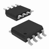
AD8350ARMZ20 Analog Devices Inc, AD8350ARMZ20 Datasheet - Page 4

AD8350ARMZ20
Manufacturer Part Number
AD8350ARMZ20
Description
IC AMP DIFF LOW-DISTORTION 8MSOP
Manufacturer
Analog Devices Inc
Datasheet
1.AD8350ARZ20-REEL7.pdf
(16 pages)
Specifications of AD8350ARMZ20
Current - Supply
28mA
Frequency
0Hz ~ 1GHz
Gain
20dB
Noise Figure
5.9dB
P1db
-2.6dBm
Package / Case
8-TSSOP, 8-MSOP (0.118", 3.00mm Width)
Rf Type
Cellular
Test Frequency
250MHz
Voltage - Supply
5 V ~ 10 V
No. Of Amplifiers
1
Input Offset Voltage
1mV
Gain Db Max
21dB
Bandwidth
0.9GHz
Slew Rate
2000V/µs
Supply Voltage Range
5V To 10V
Supply Current
28mA
Amplifier Case Style
MSOP
No. Of Pins
8
Lead Free Status / RoHS Status
Lead free / RoHS Compliant
Available stocks
Company
Part Number
Manufacturer
Quantity
Price
Part Number:
AD8350ARMZ20
Manufacturer:
ADI/亚德诺
Quantity:
20 000
Part Number:
AD8350ARMZ20-REEL7
Manufacturer:
ADI/亚德诺
Quantity:
20 000
AD8350
ABSOLUTE MAXIMUM RATINGS
Supply Voltage, V
Input Power Differential . . . . . . . . . . . . . . . . . . . . . . +8 dBm
Internal Power Dissipation . . . . . . . . . . . . . . . . . . . . 400 mW
θ
θ
Maximum Junction Temperature . . . . . . . . . . . . . . . . . 125°C
Operating Temperature Range . . . . . . . . . . . –40°C to +85°C
Storage Temperature Range . . . . . . . . . . . . –65°C to +150°C
Lead Temperature Range (Soldering 60 sec) . . . . . . . . . 300°C
Model
AD8350AR15
AD8350AR15-REEL
AD8350AR15-REEL7
AD8350ARM15
AD8350ARM15-REEL
AD8350ARM15-REEL7
AD8350AR20
AD8350AR20-REEL
AD8350AR20-REEL7
AD8350ARM20
AD8350ARM20-REEL
AD8350ARM20-REEL7
AD8350-EVAL
CAUTION
ESD (electrostatic discharge) sensitive device. Electrostatic charges as high as 4000 V readily
accumulate on the human body and test equipment and can discharge without detection. Although
the AD8350 features proprietary ESD protection circuitry, permanent damage may occur on
devices subjected to high-energy electrostatic discharges. Therefore, proper ESD precautions are
recommended to avoid performance degradation or loss of functionality.
Stresses above those listed under Absolute Maximum Ratings may cause perma-
nent damage to the device. This is a stress rating only; functional operation of the
device at these or any other conditions above those indicated in the operational
section of this specification is not implied. Exposure to absolute maximum rating
conditions for extended periods may affect device reliability.
JA
JA
SOIC (R) . . . . . . . . . . . . . . . . . . . . . . . . . . . . . . . 100°C/W
µSOIC (RM) . . . . . . . . . . . . . . . . . . . . . . . . . . . . 133°C/W
S
PIN CONFIGURATION
ENBL
OUT+
. . . . . . . . . . . . . . . . . . . . . . . . . . . . . 11 V
V
IN+
CC
1
2
3
4
(Not to Scale)
AD8350
TOP VIEW
Temperature Range
–40°C to +85°C
–40°C to +85°C
–40°C to +85°C
–40°C to +85°C
–40°C to +85°C
–40°C to +85°C
–40°C to +85°C
–40°C to +85°C
–40°C to +85°C
–40°C to +85°C
–40°C to +85°C
–40°C to +85°C
8
7
6
5
IN–
GND
GND
OUT–
ORDERING GUIDE
Package Description
8-Lead SOIC
8-Lead SOIC 13" Reel
8-Lead SOIC 7" Reel
8-Lead microSOIC
8-Lead microSOIC 13" Reel
8-Lead microSOIC 7" Reel
8-Lead SOIC
8-Lead SOIC 13" Reel
8-Lead SOIC 7" Reel
8-Lead microSOIC
8-Lead microSOIC 13" Reel
8-Lead microSOIC 7" Reel
SOIC Evaluation Board
Pin
1, 8
2
3
4, 5
6, 7
Function
IN+, IN–
ENBL
V
OUT+, OUT–
GND
CC
PIN FUNCTION DESCRIPTIONS
Description
Differential Inputs. IN+ and IN–
should be ac-coupled (pins have a dc
bias of midsupply). Differential input
impedance is 200 Ω.
Power-up Pin. A high level (5 V) enables
the device; a low level (0 V) puts device
in sleep mode.
Positive Supply Voltage. 5 V to 10 V.
Differential Outputs. OUT+ and
OUT– should be ac-coupled (pins have
a dc bias of midsupply). Differential
input impedance is 200 Ω.
Common External Ground Reference.
Package Option
SO-8
SO-8
SO-8
RM-8
RM-8
RM-8
SO-8
SO-8
SO-8
RM-8
RM-8
RM-8
WARNING!
ESD SENSITIVE DEVICE
Brand Code
Standard
Standard
Standard
J2N
J2N
J2N
Standard
Standard
Standard
J2P
J2P
J2P


