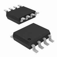
AD8350ARMZ20 Analog Devices Inc, AD8350ARMZ20 Datasheet - Page 9

AD8350ARMZ20
Manufacturer Part Number
AD8350ARMZ20
Description
IC AMP DIFF LOW-DISTORTION 8MSOP
Manufacturer
Analog Devices Inc
Datasheet
1.AD8350ARZ20-REEL7.pdf
(16 pages)
Specifications of AD8350ARMZ20
Current - Supply
28mA
Frequency
0Hz ~ 1GHz
Gain
20dB
Noise Figure
5.9dB
P1db
-2.6dBm
Package / Case
8-TSSOP, 8-MSOP (0.118", 3.00mm Width)
Rf Type
Cellular
Test Frequency
250MHz
Voltage - Supply
5 V ~ 10 V
No. Of Amplifiers
1
Input Offset Voltage
1mV
Gain Db Max
21dB
Bandwidth
0.9GHz
Slew Rate
2000V/µs
Supply Voltage Range
5V To 10V
Supply Current
28mA
Amplifier Case Style
MSOP
No. Of Pins
8
Lead Free Status / RoHS Status
Lead free / RoHS Compliant
Available stocks
Company
Part Number
Manufacturer
Quantity
Price
Part Number:
AD8350ARMZ20
Manufacturer:
ADI/亚德诺
Quantity:
20 000
Part Number:
AD8350ARMZ20-REEL7
Manufacturer:
ADI/亚德诺
Quantity:
20 000
For the output matching network, if the output source resis-
tance of the AD8350 is greater than the terminating load
resistance, a step-down network should be employed as shown
on the output of Figure 3. For a step-down matching network,
the series and parallel reactances are calculated as:
For a 10 MHz application with the 200 Ω output source resistance
of the AD8350, R
50 Ω, then X
the following component values:
The same results can be obtained using the plots in Figure 5
and Figure 6. Figure 5 shows the normalized shunt reactance
versus the normalized source resistance for a step-up matching
network, R
can be found for a given value of R
is then calculated using X
can be used to design the step-down matching network using
Figure 6.
X
S
=
C
3.2
2.8
2.6
2.4
2.2
1.8
1.6
1.4
1.2
0.8
0.6
0.4
0.2
R
3
2
P
2
1
0
S
L
S
= (2 π × 10 × 10
S
< R
×
X
NORMALIZED SOURCE RESISTANCE – R
P
NORMALIZED SOURCE RESISTANCE – R
= 86.6 × (2 π × 10 × 10
R
P
= 115.5 Ω and X
R
LOAD
LOAD
SOURCE
R
S
SOURCE
= 200 Ω, and a 50 Ω load termination, R
. By inspection, the appropriate reactance
where
X
P
S
X
= R
S
X
6
X
S
X
× 115.5)
P
S
P
R
=
S
R
LOAD
= 86.6 Ω, which results in
LOAD
S
R
R
/R
LOAD
S
LOAD
×
6
/X
–1
)
–1
P.
= 138 pF and
R
= 1.38 µH
. The series reactance
The same technique
SOURCE
S
SOURCE
R
–
LOAD
R
/R
LOAD
/R
LOAD
LOAD
LOAD
(2)
=
The same results could be found using a Smith Chart as shown
in Figure 7. In this example, a shunt capacitor and a series inductor
are used to match the 200 Ω source to a 50 Ω load. For a fre-
quency of 10 MHz, the same capacitor and inductor values
previously found using the resonant approach will transform the
200 Ω source to match the 50 Ω load. At frequencies exceeding
100 MHz, the S parameters from Tables II and III should be
used to account for the complex impedance relationships.
After determining the matching network for the single-ended
equivalent circuit, the matching elements need to be applied in a
differential manner. The series reactance needs to be split such
that the final network is balanced. In the previous examples, this
simply translates to splitting the series inductor into two equal
halves as shown in Figure 3.
Gain Adjustment
The effective gain of the AD8350 can be reduced using a num-
ber of techniques. Obviously a matched attenuator network will
reduce the effective gain, but this requires the addition of a
separate component which can be prohibitive in size and cost.
The attenuator will also increase the effective noise figure resulting
in an SNR degradation. A simple voltage divider can be imple-
mented using the combination of the driving impedance of the
previous stage and a shunt resistor across the inputs of the AD8350
as shown in Figure 8. This provides a compact solution but
suffers from an increased noise spectral density at the input
of the AD8350 due to the thermal noise contribution of the
shunt resistor. The input impedance can be dynamically altered
through the use of feedback resistors as shown in Figure 9. This
will result in a similar attenuation of the input signal by virtue
of the voltage divider established from the driving source imped-
ance and the reduced input impedance of the AD8350. Yet
this technique does not significantly degrade the SNR with
the unnecessary increase in thermal noise that arises from a truly
resistive attenuator network.
SERIES L
LOAD
SOURCE
SHUNT C
AD8350


