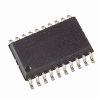
ATA3742P3-TGSY Atmel, ATA3742P3-TGSY Datasheet - Page 23

ATA3742P3-TGSY
Manufacturer Part Number
ATA3742P3-TGSY
Description
IC UHF ASK/FSK RECEIVER 20SOIC
Manufacturer
Atmel
Datasheet
1.ATA3742P3-TGQY.pdf
(34 pages)
Specifications of ATA3742P3-TGSY
Frequency
310MHz ~ 440MHz
Sensitivity
-108dBm
Data Rate - Maximum
10 kBaud
Modulation Or Protocol
ASK, FSK
Applications
RKE, TPM, Security Systems
Current - Receiving
7mA
Data Interface
PCB, Surface Mount
Antenna Connector
PCB, Surface Mount
Voltage - Supply
4.5 V ~ 5.5 V
Operating Temperature
-40°C ~ 105°C
Package / Case
20-SOIC (0.300", 7.50mm Width)
Operating Frequency (max)
450000kHz
Operating Temperature (min)
-40C
Operating Temperature (max)
105C
Operating Temperature Classification
Industrial
Operating Supply Voltage (min)
4.5V
Operating Supply Voltage (typ)
5V
Operating Supply Voltage (max)
5.5V
Lead Free Status / RoHS Status
Lead free / RoHS Compliant
Features
-
Memory Size
-
Lead Free Status / Rohs Status
Compliant
Table 5-9.
5.4.1
4900B–RKE–11/07
0
0
0
0
1
1
1
.
.
.
.
.
.
Conservation of the Register Information
Lim_max < 12 is not applicable
0
0
0
1
1
1
1
.
.
.
.
.
.
Effect of the Configuration Word Lim_max
1
1
1
1
1
1
1
.
.
.
.
.
.
Lim_max
The ATA3742 has an integrated power-on reset (POR) and brown-out detection circuitry to pro-
vide a mechanism to preserve the RAM register information.
According to
threshold voltage V
ters in that condition. Once V
period t
To indicate that condition, the receiver displays a reset marker (RM) at pin DATA after a reset.
The RM is represented by the fixed frequency f
an “L” pulse t
By means of that mechanism, the receiver cannot lose its register information without communi-
cating that condition via the reset marker RM.
• f
• If the receiver is set back to polling mode via pin DATA, RM cannot be cancelled by accident
misinterpreted by the connected microcontroller.
if t
Register” on page
RM
1
1
1
1
0
1
1
1
.
.
.
.
.
.
is lower than the lowest feasible frequency of a data signal. This means, RM cannot be
is applied according to the proposal in the Section
Rst
. A POR is also generated when the supply voltage of the receiver is turned on.
Figure
1
at pin DATA. The RM implies the following characteristics:
0
0
1
0
0
1
1
.
.
.
.
.
.
ThReset
5-13, a power-on reset is generated if the supply voltage V
24.
0
1
0
0
1
0
1
. The default parameters are programmed into the configuration regis-
.
.
.
.
.
.
S
exceeds V
(USA: T
ThReset
(T
Lim_max
Lim_max
RM
Upper Limit Value for Bit Check
, the POR is canceled after the minimum reset
at a 50% duty cycle. RM can be canceled via
= (Lim_max
= 375 µs, Europe: T
“Programming the Configuration
24 (Default)
12
13
14
61
62
63
.
.
.
.
.
.
–
1)
XLim
Lim_max
= 381 µs)
T
S
ATA3742
Clk
drops below the
)
23


