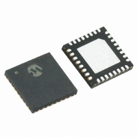
MRF89XA-I/MQ Microchip Technology, MRF89XA-I/MQ Datasheet - Page 22

MRF89XA-I/MQ
Manufacturer Part Number
MRF89XA-I/MQ
Description
TXRX ISM SUB-GHZ ULP 32QFN
Manufacturer
Microchip Technology
Specifications of MRF89XA-I/MQ
Package / Case
32-WFQFN Exposed Pad
Frequency
863MHz ~ 870MHz, 902MHz ~ 928MHz, 950MHz ~ 960MHz
Data Rate - Maximum
200kbps
Modulation Or Protocol
FSK, OOK
Applications
ISM
Power - Output
12.5dBm
Sensitivity
-113dBm
Voltage - Supply
2.1 V ~ 3.6 V
Current - Receiving
3mA
Current - Transmitting
25mA
Data Interface
PCB, Surface Mount
Antenna Connector
PCB, Surface Mount
Operating Temperature
-40°C ~ 85°C
Number Of Receivers
1
Number Of Transmitters
1
Wireless Frequency
863 MHz to 870 MHz, 902 MHz to 928 MHz, 950 MHz to 960 MHz
Interface Type
SPI
Noise Figure
- 112 dBc
Output Power
- 8.5 dBm, + 12.5 dBm
Operating Supply Voltage
2.1 V to 3.6 V
Maximum Operating Temperature
+ 85 C
Mounting Style
SMD/SMT
Maximum Data Rate
256 Kbps
Maximum Supply Current
25 mA
Minimum Operating Temperature
- 40 C
Modulation
FSK
Lead Free Status / RoHS Status
Lead free / RoHS Compliant
Memory Size
-
Lead Free Status / Rohs Status
Lead free / RoHS Compliant
Available stocks
Company
Part Number
Manufacturer
Quantity
Price
Company:
Part Number:
MRF89XA-I/MQ
Manufacturer:
MICROCHIP
Quantity:
12 000
FIGURE 2-9:
FIGURE 2-10:
2.11
The
microcontroller through a 4-wire SPI port as a slave
device. An SPI-compatible serial interface allows the
user to select, command and monitor the status of the
MRF89XA through the host microcontroller. All
registers are addressed through specific addresses to
control, configure and read status bytes.
FIGURE 2-11:
DS70622B-page 22
MRF89XA
in FSK mode
equal to f
IF2 < 0
in FSK mode
MRF89XA
IF2 = 0
Serial Peripheral Interface (SPI)
0
Configuration
Registers
o
Registers
down-conversion
Config.
FIFO
0
down-conversion
Second
Second
communicates
Approx. 100 MHz
FSK RECEIVER SETTING
OOK RECEIVER SETTING
SPI OVERVIEW AND HOST MICROCONTROLLER CONNECTIONS
MRF89XA
LO2
IF1
RX
100 MHz
Approx.
IF1
LO2 RX
with
CONFIG
(Slave)
(Slave)
DATA
SPI
SPI
the
host
Preliminary
down-conversion
CSCON
SDI
SDO
SCK
CSDAT
down-conversion
First
The SPI in the MRF89XA consists of the following two
sub-blocks, as illustrated in Figure 2-11:
• SPI CONFIG: This sub-block is used in all data
• SPI DATA: This sub-block is used in Buffered and
First
operation modes to read and write the configuration
registers which control all the parameters of the chip
(operating mode, frequency and bit rate).
Packet mode to write and read data bytes to and
from the FIFO. (FIFO Interrupts can be used to
manage the FIFO content).
Frequency
Image
Frequency
Image
I/O
SDI
SDO
SCK
I/O
© 2010 Microchip Technology Inc.
LO1 RX
LO1 RX
PIC
®
Microcontroller
(Master)
Channel
Channel
Frequency
Frequency


