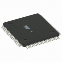
ATMEGA256RZBV-8AU Atmel, ATMEGA256RZBV-8AU Datasheet - Page 161

ATMEGA256RZBV-8AU
Manufacturer Part Number
ATMEGA256RZBV-8AU
Description
MCU ATMEGA2560/AT86RF230 100TQFP
Manufacturer
Atmel
Series
ATMEGAr
Datasheets
1.ATMEGA640V-8CU.pdf
(38 pages)
2.ATMEGA640V-8CU.pdf
(444 pages)
3.AT86RF230-ZU.pdf
(98 pages)
Specifications of ATMEGA256RZBV-8AU
Frequency
2.4GHz
Modulation Or Protocol
802.15.4 Zigbee
Applications
ISM, ZigBee™
Power - Output
3dBm
Sensitivity
-101dBm
Voltage - Supply
1.8 V ~ 3.6 V
Current - Receiving
15.5mA
Current - Transmitting
16.5mA
Data Interface
PCB, Surface Mount
Memory Size
256kB Flash, 4kB EEPROM, 8kB RAM
Antenna Connector
PCB, Surface Mount
Package / Case
100-TQFP
Wireless Frequency
2.4 GHz
Interface Type
JTAG, SPI
Output Power
3 dBm
Operating Temperature Range
- 55 C to + 125 C
For Use With
ATAVRISP2 - PROGRAMMER AVR IN SYSTEMATJTAGICE2 - AVR ON-CHIP D-BUG SYSTEM
Lead Free Status / RoHS Status
Lead free / RoHS Compliant
Operating Temperature
-
Data Rate - Maximum
-
Lead Free Status / Rohs Status
Lead free / RoHS Compliant
For Use With/related Products
ATmega256
- Current page: 161 of 444
- Download datasheet (10Mb)
16.11.9
2549M–AVR–09/10
TCCR1C – Timer/Counter 1 Control Register C
• Bit 6 – ICESn: Input Capture Edge Select
This bit selects which edge on the Input Capture Pin (ICPn) that is used to trigger a capture
event. When the ICESn bit is written to zero, a falling (negative) edge is used as trigger, and
when the ICESn bit is written to one, a rising (positive) edge will trigger the capture.
When a capture is triggered according to the ICESn setting, the counter value is copied into the
Input Capture Register (ICRn). The event will also set the Input Capture Flag (ICFn), and this
can be used to cause an Input Capture Interrupt, if this interrupt is enabled.
When the ICRn is used as TOP value (see description of the WGMn3:0 bits located in the
TCCRnA and the TCCRnB Register), the ICPn is disconnected and consequently the input cap-
ture function is disabled.
• Bit 5 – Reserved Bit
This bit is reserved for future use. For ensuring compatibility with future devices, this bit must be
written to zero when TCCRnB is written.
• Bit 4:3 – WGMn3:2: Waveform Generation Mode
See TCCRnA Register description.
• Bit 2:0 – CSn2:0: Clock Select
The three clock select bits select the clock source to be used by the Timer/Counter, see
16-10 on page 156
Table 16-6.
If external pin modes are used for the Timer/Countern, transitions on the Tn pin will clock the
counter even if the pin is configured as an output. This feature allows software control of the
counting.
Bit
(0x82)
Read/Write
Initial Value
CSn2
0
0
0
0
1
1
1
1
CSn1
0
0
1
1
0
0
1
1
Clock Select Bit Description
FOC1A
W
7
0
and
CSn0
Figure 16-11 on page
FOC1B
0
1
0
1
0
1
0
1
W
6
0
ATmega640/1280/1281/2560/2561
FOC1C
W
5
0
External clock source on Tn pin. Clock on falling edge
External clock source on Tn pin. Clock on rising edge
No clock source. (Timer/Counter stopped)
R
4
–
0
156.
clk
clk
clk
clk
I/O
clk
R
I/O
3
–
0
I/O
I/O
/1024 (From prescaler)
/256 (From prescaler)
I/O
/64 (From prescaler)
/8 (From prescaler)
Description
/1 (No prescaling
R
2
–
0
R
1
0
–
R
0
–
0
TCCR1C
Figure
161
Related parts for ATMEGA256RZBV-8AU
Image
Part Number
Description
Manufacturer
Datasheet
Request
R

Part Number:
Description:
DEV KIT FOR AVR/AVR32
Manufacturer:
Atmel
Datasheet:

Part Number:
Description:
INTERVAL AND WIPE/WASH WIPER CONTROL IC WITH DELAY
Manufacturer:
ATMEL Corporation
Datasheet:

Part Number:
Description:
Low-Voltage Voice-Switched IC for Hands-Free Operation
Manufacturer:
ATMEL Corporation
Datasheet:

Part Number:
Description:
MONOLITHIC INTEGRATED FEATUREPHONE CIRCUIT
Manufacturer:
ATMEL Corporation
Datasheet:

Part Number:
Description:
AM-FM Receiver IC U4255BM-M
Manufacturer:
ATMEL Corporation
Datasheet:

Part Number:
Description:
Monolithic Integrated Feature Phone Circuit
Manufacturer:
ATMEL Corporation
Datasheet:

Part Number:
Description:
Multistandard Video-IF and Quasi Parallel Sound Processing
Manufacturer:
ATMEL Corporation
Datasheet:

Part Number:
Description:
High-performance EE PLD
Manufacturer:
ATMEL Corporation
Datasheet:

Part Number:
Description:
8-bit Flash Microcontroller
Manufacturer:
ATMEL Corporation
Datasheet:

Part Number:
Description:
2-Wire Serial EEPROM
Manufacturer:
ATMEL Corporation
Datasheet:


