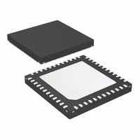
ATA5423-PLSW Atmel, ATA5423-PLSW Datasheet - Page 74

ATA5423-PLSW
Manufacturer Part Number
ATA5423-PLSW
Description
IC TXRX ASK/FSK 315MHZ 48QFN
Manufacturer
Atmel
Specifications of ATA5423-PLSW
Frequency
315MHz
Data Rate - Maximum
20kbps
Modulation Or Protocol
ASK, FSK
Applications
Alarm, ISM, Telemetry
Power - Output
5dBm
Sensitivity
-112.5dBm
Voltage - Supply
2.4 V ~ 3.6 V or 4.4 V ~ 6.6 V
Current - Receiving
10.5mA
Current - Transmitting
10mA
Data Interface
PCB, Surface Mount
Antenna Connector
PCB, Surface Mount
Operating Temperature
-40°C ~ 85°C
Package / Case
48-VQFN Exposed Pad, 48-HVQFN, 48-SQFN, 48-DHVQFN
Lead Free Status / RoHS Status
Lead free / RoHS Compliant
Memory Size
-
12. Electrical Characteristics: General (Continued)
This device is manufactured with an industrial (not automotive) grade process and process controls. Although this device may
meet certain automotive grade criteria in performance, Atmel can not recommend that this device be used in any automotive
application.
All parameters refer to GND and are valid for T
and V
about current consumption, timing and digital pin properties can be found in the specific sections of the “Electrical Characteristics”.
74
*) Type means: A = 100% tested, B = 100% correlation tested, C = Characterized on samples, D = Design parameter
Note:
No. Parameters
3.1
3.2 Output power 1
3.3
3
VS2
Power Amplifier/TX Mode
Supply current TX mode
power amplifier OFF
Supply current TX mode
power amplifier ON 1
= V
1. Pin numbers in brackets mean they were measured with RF_IN matched to 50 according to
ATA5423/ATA5425/ATA5428/ATA5429
VAUX
component values according to
with component values according to
= 5.0V (Base
-
station Application). Typical values are given at f
Test Conditions
f
f
f
f
f
V
T
V
f
R
R
f
R
R
f
R
R
f
R
R
f
R
R
RF_OUT matched to
R
j/(2
PA on/0 dBm
f
f
f
f
f
RF
RF
RF
RF
RF
RF
RF
RF
RF
RF
RF
RF
RF
RF
RF
amb
VS1
PWR_H
R_PWR
Lopt
R_PWR
Lopt
R_PWR
Lopt
R_PWR
Lopt
R_PWR
Lopt
Lopt
= 868.3 MHz
= 915 MHz
= 315 MHz
= 345 MHz
= 433.92 MHz
= 315 MHz
= 345 MHz
= 433.92 MHz
= 868.3 MHz
= 915 MHz
= 315 MHz
= 345 MHz
= 433.92 MHz
= 868.3 MHz
= 915 MHz
= V
= 25°C
= 2.5 k
= 2.4 k
= 2.3 k
= 1.3 k
= 1.1 k
//
= 0V
= 56 k
= 56 k
= 56 k
= 30 k
= 33 k
VS2
f
Table 3-2 on page 12
RF
= 3V
amb
Table 3-7 on page
= 25°C, V
1.0 pF
VS1
17, 18
17, 18
17, 18
17, 18
17, 18
Pin
(10)
= V
(1)
VS2
and RF_OUT matched to 50 according to
22.
= 3.0V (1
I
I
I
I
I
I
I
S_TX_PAON1
S_TX_PAON1
S_TX_PAON1
S_TX_PAON1
S_TX_PAON1
S_TX_PAOFF
S_TX_PAOFF
Symbol
P
REF1
-
RF
battery application), V
= 433.92 MHz unless otherwise specified. Details
Min.
–
2.5
Typ.
6.50
6.95
8.5
8.6
8.6
9.6
9.6
0
VS2
= 6.0V (2-battery application)
Figure 3-1 on page 11
Figure 3-10 on page 21
Max.
+2.5
4841D–WIRE–10/07
dBm
Unit
mA
mA
mA
mA
mA
mA
mA
Type*
with
A
A
B
B
B
B
B
B


