AT86RF211DAI Atmel, AT86RF211DAI Datasheet - Page 7
AT86RF211DAI
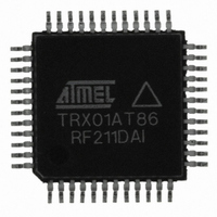
Manufacturer Part Number
AT86RF211DAI
Description
IC RF TXRX FSK 400-950MHZ 48TQFP
Manufacturer
Atmel
Datasheet
1.AT86RF211DB-433LT.pdf
(19 pages)
Specifications of AT86RF211DAI
Frequency
400MHz ~ 950MHz
Data Rate - Maximum
100kbps
Modulation Or Protocol
FSK
Applications
ISM
Power - Output
7dBm ~ 12dBm
Sensitivity
-107dBm
Voltage - Supply
2.4 V ~ 3.6 V
Data Interface
PCB, Surface Mount
Antenna Connector
PCB, Surface Mount
Operating Temperature
-40°C ~ 85°C
Package / Case
48-TQFP Exposed Pad, 48-eTQFP, 48-HTQFP, 48-VQFP
Lead Free Status / RoHS Status
Contains lead / RoHS non-compliant
Memory Size
-
Current - Transmitting
-
Current - Receiving
-


Encoding Scheme for the
Data/Address Fields
Loop Filter
2186A–WIRE–08/02
-2400 bits/s
-4800 bits/s
-9600 bits/s
Max. number of consecutive "0" or "1"
5
10
20
Atmel recommends:
•
•
About the Charge of the Capacitor:
•
•
•
•
The duty cycle in the Address and the Data field can be as flexible as 30/70% or 70/30%
(so meeting the header duty cycle requirement is OK for the rest of the message).
However, in order to keep the SKFILT capacitor charged at a correct level during the
Address & Data fields (62 bits), one must not exceed a maximum number of equal con-
secutive bits, and "balance" the number of "0" and "1" as follow:
In any case, the discriminator of the AT86RF211 does NOT require a Manchester
encoding.
The loop filter of the PLL acts on the spectrum occupancy, the phase noise of the RF
signal, the shape of the modulation, the rising and falling edges of the modulated signal
of the transmitter (transitions between F0 and F1), the demodulated signal on the
receiver (DISCOUT signal). In order to meet the duty cycle tolerance, the rising and fall-
ing edges of the demodulated signals must be sharp enough, especially when the data
rate grows.
The ''External'' Mode for the Data Slicer: since the demodulated signal is
compared to its average value, stored into an external capacitor, the duty cycle
remains naturally very close to 50% even if the external conditions (i.e. temperature)
have changed between two wake-up timeslots, with no need for data slicer
threshold re-adjustment.
A Value of SKFILT = 22 nF to meet the duty cycle requirements from 1 to 10
kbits/s.
the user must make sure that the SKFILT capacitor is charged before the
recognition of the header starts (since the header recognition is based on re-shaped
data). The maximum charging time is 15 ms (from 0V) with 22 nF.
the SKFILT pin is set into a very high impedance state when the device is in the
"sleep" phase. For SKFILT = 22 nF, the discharge is about 200 mV for WPER =
60 s, and 1V for WPER = 6 minutes. For WPER < 1 min, there is no need to
recharge the capacitor to be able to re-start the header recognition. Above 1
minute, an additional relevant charging time (depending on WPER) must be taken
into account within WL2.
no need for the capacitor to be at the right value at the end of WL1: keeping WL1 as
short as possible is important to keep the average power consumption as low as
possible.
WL1 = 2 ms and WL2 = 4 ms are the minimum values to make sure that the wake-
up will operate properly.
Any frame of this length must be "balanced" (= as many "0" as "1")
10
20
40
AT86RF211 (TRX01)
7
Related parts for AT86RF211DAI
Image
Part Number
Description
Manufacturer
Datasheet
Request
R

Part Number:
Description:
DEV KIT FOR AVR/AVR32
Manufacturer:
Atmel
Datasheet:

Part Number:
Description:
INTERVAL AND WIPE/WASH WIPER CONTROL IC WITH DELAY
Manufacturer:
ATMEL Corporation
Datasheet:
Part Number:
Description:
Low-Voltage Voice-Switched IC for Hands-Free Operation
Manufacturer:
ATMEL Corporation
Datasheet:
Part Number:
Description:
MONOLITHIC INTEGRATED FEATUREPHONE CIRCUIT
Manufacturer:
ATMEL Corporation
Datasheet:
Part Number:
Description:
AM-FM Receiver IC U4255BM-M
Manufacturer:
ATMEL Corporation
Datasheet:
Part Number:
Description:
Monolithic Integrated Feature Phone Circuit
Manufacturer:
ATMEL Corporation
Datasheet:
Part Number:
Description:
Multistandard Video-IF and Quasi Parallel Sound Processing
Manufacturer:
ATMEL Corporation
Datasheet:
Part Number:
Description:
High-performance EE PLD
Manufacturer:
ATMEL Corporation
Datasheet:
Part Number:
Description:
8-bit Flash Microcontroller
Manufacturer:
ATMEL Corporation
Datasheet:
Part Number:
Description:
2-Wire Serial EEPROM
Manufacturer:
ATMEL Corporation
Datasheet: