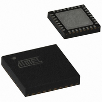
ATR2406-PNSG Atmel, ATR2406-PNSG Datasheet - Page 13

ATR2406-PNSG
Manufacturer Part Number
ATR2406-PNSG
Description
IC IF ISM TXRX 2.4GHZ 32QFN
Manufacturer
Atmel
Datasheet
1.ATR2406-DEV-BOARD.pdf
(25 pages)
Specifications of ATR2406-PNSG
Frequency
2.4GHz
Data Rate - Maximum
1.152Mbps
Modulation Or Protocol
DSSS, GFSK
Applications
Wireless Game Controllers
Power - Output
4dBm
Sensitivity
-93dBm
Voltage - Supply
2.9 V ~ 3.6 V
Current - Receiving
57mA
Current - Transmitting
42mA
Data Interface
PCB, Surface Mount
Antenna Connector
PCB, Surface Mount
Operating Temperature
-10°C ~ 60°C
Package / Case
32-VQFN Exposed Pad, 32-HVQFN, 32-SQFN, 32-DHVQFN
Lead Free Status / RoHS Status
Contains lead / RoHS non-compliant
Memory Size
-
Other names
ATR2406-PNSGCT
ATR2406-PNSGCT
ATR2406-PNSGCT
Available stocks
Company
Part Number
Manufacturer
Quantity
Price
Part Number:
ATR2406-PNSG
Manufacturer:
ATMEL/爱特梅尔
Quantity:
20 000
7.7
7.8
7.9
Figure 7-2.
4779N–ISM–12/08
Control Signals
Serial Programming Bus
3-wire Bus Timing
ENABLE
CLOCK
DATA
3-wire Bus Protocol Timing Diagram
TL
The various transceiver functions are activated by the following control signals. A timing pro-
posal is shown in
Table 7-7.
The transceiver is programmed by the SPI (CLOCK, DATA and ENABLE).
After setting the enable signal to low, the data is transferred bit by bit into the shift register on the
rising edge of the clock signal, starting with the MSBit. When the enable signal has returned to
high, the programmed information is active. Additional leading bits are ignored and there is no
check made of how many clock pulses arrived during enable low.
The programming of the transceiver is done by a 16-bit or 25-bit data word (for the RX clock
recovery mode).
Table 7-8.
Description
Clock period
Set time data to clock
Hold time data to clock
Clock pulse width
Set time enable to clock
Hold time enable to data
Time between two protocols
PU_REG
PU_TRX
RX_ON
TX_ON
Signal
nOLE
Control Signals and Functions
3-wire Bus Protocol Table
Figure 7-3 on page 14
Functions
Activates AUX voltage regulator and the VCO voltage regulator supplying the
complete transceiver
Activates RX/TX blocks
Activates RX circuits: DEMOD, IF AMP, IR MIXER
Activates TX circuits: PA, RAMP GEN, Starts RAMP SIGNAL at RAMP_OUT
Disables open loop mode of the PLL
TPER
TS
TC
TH
Symbol
TPER
TEC
TS
TH
TC
TT
TL
Minimum Value
TEC
100
100
250
20
20
60
0
TT
ATR2406
Unit
ns
ns
ns
ns
ns
ns
ns
13


