ATR2406-PNSG Atmel, ATR2406-PNSG Datasheet - Page 8
ATR2406-PNSG
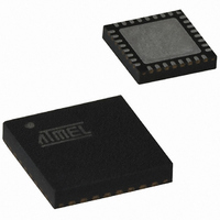
Manufacturer Part Number
ATR2406-PNSG
Description
IC IF ISM TXRX 2.4GHZ 32QFN
Manufacturer
Atmel
Datasheet
1.ATR2406-DEV-BOARD.pdf
(25 pages)
Specifications of ATR2406-PNSG
Frequency
2.4GHz
Data Rate - Maximum
1.152Mbps
Modulation Or Protocol
DSSS, GFSK
Applications
Wireless Game Controllers
Power - Output
4dBm
Sensitivity
-93dBm
Voltage - Supply
2.9 V ~ 3.6 V
Current - Receiving
57mA
Current - Transmitting
42mA
Data Interface
PCB, Surface Mount
Antenna Connector
PCB, Surface Mount
Operating Temperature
-10°C ~ 60°C
Package / Case
32-VQFN Exposed Pad, 32-HVQFN, 32-SQFN, 32-DHVQFN
Lead Free Status / RoHS Status
Contains lead / RoHS non-compliant
Memory Size
-
Other names
ATR2406-PNSGCT
ATR2406-PNSGCT
ATR2406-PNSGCT
Available stocks
Company
Part Number
Manufacturer
Quantity
Price

Part Number:
ATR2406-PNSG
Manufacturer:
ATMEL/爱特梅尔
Quantity:
20 000


6. Electrical Characteristics (Continued)
V
8
Notes:
S
10.1 Charge-pump output current
10.2 Leakage current
11.1 Transmit to receive time
11.2 Receive to transmit time
11.3 Channel switch time
11.4 Power down to transmit
11.5 Power down to receive
11.6 Programming register
11.7 PLL settling time
12.1 HIGH-level input voltage
12.2 LOW-level input voltage
12.3 HIGH-level output voltage
12.4 LOW-level output voltage
12.5 Input bias current
12.6 3-wire bus clock frequency
No.
8.1
8.2
8.3
8.4
8.5
9.1
10
11
12
= 3.6V with AUX regulator, T
8
9
Parameters
Synthesizer
External reference input
frequency
Sinusoidal input signal level
(peak-to-peak value)
Scaling factor prescaler
Scaling factor main counter
Scaling factor swallow counter
Phase Detector
Phase detector comparison
frequency
Charge-pump Output
Timing Conditions
Interface Logic Input and Output Signal Levels, Pin DATA, CLOCK, ENABLE
1. Measured and guaranteed only on the Atmel
2. Timing is determined by external loop filter characteristics. Faster timing can be achieved by modification of the loop filter.
3. The Gaussian filter control setting (GFCS) is used to compensate production tolerances by tuning the modulation deviation
4. Burst mode with 0.9% duty cycle
ATR2406
quency (Smart RF) firmware. Conducted measured.
For further information refer to the application notes.
in production to the nominal value of 400 kHz.
(1)(2)
amb
= 25°C, unless otherwise specified
Test Conditions
D7 = 0
D7 = 1
AC-coupled sine wave
V
V
Reference clock stable
Reference clock stable
Reference clock stable
Reference clock stable
Reference clock stable
Reference clock stable
Reference clock stable
Logic 1
Logic 0
Logic 1
Logic 0
Logic 1 or logic 0
CP
CP
= 1/2 V
= 1/2 V
CC
CC
®
evaluation board, including microstrip filter, balun, and Smart Radio Fre-
PD
TX
RX
PD
PLL set time
REF_CLK
REF_CLK
PRR time
Symbol
CS time
f
CLKmax
S
S
V
S
V
I
f
I
V
V
bias
PSC
RX time
RX time
PD
CP
I
TX time
TR time
MC
OH
SC
OL
L
IH
IL
Min.
–0.3
500
1.4
–5
0
0
86/87/88/89
10.368
13.824
32/33
1728
±100
Typ.
200
200
200
250
200
200
±2
3
Max.
1000
1000
+0.4
3.1
3.1
+5
31
10
4779N–ISM–12/08
mV
MHz
MHz
MHz
Unit
kHz
mA
pA
µA
µs
µs
µs
µs
µs
µs
µs
V
V
V
V
-
-
-
PP
Related parts for ATR2406-PNSG
Image
Part Number
Description
Manufacturer
Datasheet
Request
R

Part Number:
Description:
BOARD DEVELOPMENT FOR ATR2406
Manufacturer:
Atmel
Datasheet:

Part Number:
Description:
Atr2406 Low-if 2.4-ghz Ism Transceiver
Manufacturer:
ATMEL Corporation
Datasheet:

Part Number:
Description:
BOARD DEV FOR ATR2406/ATMEGA88
Manufacturer:
Atmel
Datasheet:

Part Number:
Description:
KIT DEMO FOR ATR2406/ATMEGA88
Manufacturer:
Atmel
Datasheet:

Part Number:
Description:
LOW IF .4 GHZ ISM TRANSCEIVER
Manufacturer:
ATMEL [ATMEL Corporation]
Datasheet:

Part Number:
Description:
RF Transceiver COM.ISM-SMART RF 2.4GHZ ISM TRX
Manufacturer:
Atmel
Datasheet:

Part Number:
Description:
Manufacturer:
Atmel
Datasheet:


Part Number:
Description:
DEV KIT FOR AVR/AVR32
Manufacturer:
Atmel
Datasheet:
Part Number:
Description:
INTERVAL AND WIPE/WASH WIPER CONTROL IC WITH DELAY
Manufacturer:
ATMEL Corporation
Datasheet:
Part Number:
Description:
Low-Voltage Voice-Switched IC for Hands-Free Operation
Manufacturer:
ATMEL Corporation
Datasheet:
Part Number:
Description:
MONOLITHIC INTEGRATED FEATUREPHONE CIRCUIT
Manufacturer:
ATMEL Corporation
Datasheet:
Part Number:
Description:
AM-FM Receiver IC U4255BM-M
Manufacturer:
ATMEL Corporation
Datasheet:
Part Number:
Description:
Monolithic Integrated Feature Phone Circuit
Manufacturer:
ATMEL Corporation
Datasheet: