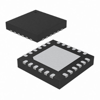
ATA8743-PXQW Atmel, ATA8743-PXQW Datasheet - Page 188

ATA8743-PXQW
Manufacturer Part Number
ATA8743-PXQW
Description
MCU W/TRANSMITTER ASK/FSK 24QFN
Manufacturer
Atmel
Datasheet
1.ATA8743-PXQW.pdf
(238 pages)
Specifications of ATA8743-PXQW
Frequency
868MHz ~ 928MHz
Applications
Home Automation, Remote Sensing, RKE
Modulation Or Protocol
ASK, FSK
Data Rate - Maximum
32 kBit/s
Power - Output
3.5dBm ~ 8dBm
Current - Transmitting
9.3mA
Data Interface
PCB, Surface Mount
Antenna Connector
PCB, Surface Mount
Memory Size
4kB Flash, 256B EEPROM, 256B SRAM
Voltage - Supply
1.8 V ~ 3.6 V
Operating Temperature
-40°C ~ 85°C
Package / Case
24-VQFN Exposed Pad, 24-HVQFN, 24-SQFN, 24-DHVQFN
Processor Series
ATA8x
Core
AVR8
Data Bus Width
8 bit
Program Memory Type
Flash
Program Memory Size
4 KB
Data Ram Size
256 B
Interface Type
SPI, USI
Maximum Clock Frequency
16 MHz
Number Of Programmable I/os
12
Number Of Timers
2
Maximum Operating Temperature
+ 85 C
Mounting Style
SMD/SMT
Development Tools By Supplier
ATASTK512-EK1-IND
Minimum Operating Temperature
- 40 C
On-chip Adc
10 bit, 8 Channel
Lead Free Status / RoHS Status
Lead free / RoHS Compliant
Features
-
Lead Free Status / Rohs Status
Details
- Current page: 188 of 238
- Download datasheet (4Mb)
28.7
188
High-voltage Serial Programming
ATA8743
This section describes how to program and verify Flash Program memory, EEPROM Data mem-
ory, Lock bits and Fuse bits in the ATtiny24/44/84.
Figure 28-3. High-voltage Serial Programming
Table 28-12. Pin Name Mapping
The minimum period for the Serial Clock Input (SCI) during High-voltage Serial Programming is
220 ns.
Table 28-13. Pin Values Used to Enter Programming Mode
Signal Name in High-voltage
Serial Programming Mode
SDI
SII
SDO
SCI
Pin
PA0
PA1
PA2
SCI
+11.5 - 12.5V
Symbol
Prog_enable[0]
Prog_enable[1]
Prog_enable[2]
PB3
PB0
GND
Pin Name
PA6
PA5
PA4
PB0
(RESET)
I/O
I
I
O
I
VCC
PA4
PA5
PA6
Function
Serial Data Input
Serial Instruction Input
Serial Data Output
Serial Clock Input (min. 220ns period)
+1.8 - 5.5V
SDO
SII
SDI
9152B–INDCO–02/10
Value
0
0
0
Related parts for ATA8743-PXQW
Image
Part Number
Description
Manufacturer
Datasheet
Request
R

Part Number:
Description:
Manufacturer:
ATMEL Corporation
Datasheet:

Part Number:
Description:
DEV KIT FOR AVR/AVR32
Manufacturer:
Atmel
Datasheet:

Part Number:
Description:
INTERVAL AND WIPE/WASH WIPER CONTROL IC WITH DELAY
Manufacturer:
ATMEL Corporation
Datasheet:

Part Number:
Description:
Low-Voltage Voice-Switched IC for Hands-Free Operation
Manufacturer:
ATMEL Corporation
Datasheet:

Part Number:
Description:
MONOLITHIC INTEGRATED FEATUREPHONE CIRCUIT
Manufacturer:
ATMEL Corporation
Datasheet:

Part Number:
Description:
AM-FM Receiver IC U4255BM-M
Manufacturer:
ATMEL Corporation
Datasheet:

Part Number:
Description:
Monolithic Integrated Feature Phone Circuit
Manufacturer:
ATMEL Corporation
Datasheet:

Part Number:
Description:
Multistandard Video-IF and Quasi Parallel Sound Processing
Manufacturer:
ATMEL Corporation
Datasheet:

Part Number:
Description:
High-performance EE PLD
Manufacturer:
ATMEL Corporation
Datasheet:

Part Number:
Description:
8-bit Flash Microcontroller
Manufacturer:
ATMEL Corporation
Datasheet:

Part Number:
Description:
2-Wire Serial EEPROM
Manufacturer:
ATMEL Corporation
Datasheet:


