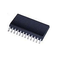
SP207EEA-L Exar Corporation, SP207EEA-L Datasheet - Page 6

SP207EEA-L
Manufacturer Part Number
SP207EEA-L
Description
IC TXRX RS232 ESD LP 24SSOP
Manufacturer
Exar Corporation
Type
Transceiverr
Datasheet
1.SP213ECA-L.pdf
(19 pages)
Specifications of SP207EEA-L
Package / Case
24-SSOP (0.200", 5.30mm Width)
Number Of Drivers/receivers
5/3
Protocol
RS232
Voltage - Supply
4.5 V ~ 5.5 V
Mounting Type
Surface Mount
On Resistance (max)
7 KOhms
Propagation Delay Time
1.5 us
Maximum Operating Temperature
+ 85 C
Minimum Operating Temperature
- 40 C
Function
Transceiver
Mounting Style
SMD/SMT
Supply Current
3 mA
Supply Voltage (max)
6 V
Supply Voltage (min)
5 V
Logic Type
RS-232 Transceivers
Number Of Circuits
3
Lead Free Status / RoHS Status
Lead free / RoHS Compliant
Lead Free Status / RoHS Status
Lead free / RoHS Compliant, Lead free / RoHS Compliant
Available stocks
Company
Part Number
Manufacturer
Quantity
Price
Company:
Part Number:
SP207EEA-L
Manufacturer:
Exar
Quantity:
135
Company:
Part Number:
SP207EEA-L
Manufacturer:
MOTOROLA
Quantity:
2 000
Company:
Part Number:
SP207EEA-L/TR
Manufacturer:
PANASONIC
Quantity:
6 219
Receiver input thresholds are between .2
to .7 volts typical. This allows the receiver
to detect standard TTL or CMOS logic-level
signals as well as RS-232 signals. If a re-
ceiver input is left unconnected or un-driven,
a 5kΩ pulldown resistor to ground will commit
the receiver to a logic- output state.
Highly Efficient Charge–Pump
The onboard dual-output charge pump is
used to generate positive and negative signal
voltages for the RS-232 drivers. This enables
fully compliant RS-232 and V.28 signals from
a single power supply device.
The charge pumps use four external capaci-
tors to hold and transfer electrical charge.
The Exar–patented design (US Patent
#5,306,954) uses a unique approach com-
pared to older, less–efficient designs. The
pumps use a four–phase voltage shifting
technique to attain symmetrical V+ and V-
power supplies. An intelligent control oscil-
lator regulates the operation of the charge
pump to maintain the proper voltages at
maximum efficiency.
Phase 1
V
terminals of capacitors C
from V
connected to ground. C
to ground and the stored charge from C
superimposed onto C
connected to V
capacitor C
SS
charge store and double — The positive
C
CC
1
Figure . Charge Pump — Phase
–5V
+
–
V
with their negative terminals initially
CC
= +5V
2
is now 2 x V
CC
Exar Corporation 48720 Kato Road, Fremont CA, 94538 • 50-668-707 • www.exar.com
C
the voltage potential across
2
+5V
–5V
+
–
2
– . Since C
l
+ is then connected
and C
CC
+
–
C
C
4
.
3
+
–
V
V
DD
SS
2
are charged
Storage Capacitor
Storage Capacitor
2
+ is still
– is
6
Phase 2
— V
nects the negative terminal of C
storage capacitor and the positive terminal
of C
and inverted (V - ) voltage onto C
capacitor C
for its next phase.
Phase 3
V
is identical to the first phase. The positive
terminals of capacitors C
from V
connected to ground. C
to ground and the stored charge from C
superimposed onto C
connected to V
capacitor C
Phase 4
V
the negative terminal of C
the positive terminal of C
age capacitor. This transfers the doubled
(V+) voltage onto C
C
next phase.
DD
DD
is charged from V
charge store and double —Phase three
2
SS
transfer — The fourth phase connects
Figure 3. Charge Pump — Phase 3
to ground. This transfers the doubled
C
C
CC
1
transfer and invert — Phase two con-
1
Figure 2. Charge Pump — Phase 2
–5V
+
–
+
–
V
V
with their negative terminals initially
CC
CC
= +5V
= +5V
2
charged from V
is now 2 x V
CC
C
C
2
2
the voltage potential across
+5V
–5V
–10V
+
+
–
–
4
. Meanwhile, capacitor
CC
2
– . Since C
l
+ is then connected
to prepare it for its
and C
CC
+
+
–
–
C
C
2
C
C
4
4
2
.
3
+
+
3
–
–
to the V
CC
to ground and
V
V
V
V
SP207E_00_072309
DD
SS
3
DD
SS
2
. Meanwhile,
to prepare it
are charged
Storage Capacitor
Storage Capacitor
Storage Capacitor
Storage Capacitor
2
to the V
2
+ is still
DD
stor-
– is
SS


