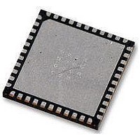
AT89LP52-20MU Atmel, AT89LP52-20MU Datasheet - Page 19

AT89LP52-20MU
Manufacturer Part Number
AT89LP52-20MU
Description
IC MCU 8051 8K FLASH SPI 44VQFN
Manufacturer
Atmel
Series
89LPr
Datasheet
1.AT89LP52-20MU.pdf
(113 pages)
Specifications of AT89LP52-20MU
Core Processor
8051
Core Size
8-Bit
Speed
20MHz
Connectivity
EBI/EMI, I²C, SPI, UART/USART
Peripherals
Brown-out Detect/Reset, POR, PWM, WDT
Number Of I /o
36
Program Memory Size
8KB (8K x 8)
Program Memory Type
FLASH
Ram Size
256 x 8
Voltage - Supply (vcc/vdd)
2.4 V ~ 5.5 V
Oscillator Type
Internal
Operating Temperature
-40°C ~ 85°C
Package / Case
44-VFQFN Exposed Pad
Processor Series
AT89x
Core
8051
Data Bus Width
8 bit
Data Ram Size
256 B
Interface Type
Serial
Maximum Clock Frequency
20 MHz
Number Of Programmable I/os
36
Number Of Timers
3
Operating Supply Voltage
2.7 V to 5.5 V
Maximum Operating Temperature
+ 85 C
Mounting Style
SMD/SMT
Lead Free Status / RoHS Status
Lead free / RoHS Compliant
Eeprom Size
-
Data Converters
-
Lead Free Status / Rohs Status
Details
Available stocks
Company
Part Number
Manufacturer
Quantity
Price
Company:
Part Number:
AT89LP52-20MU
Manufacturer:
Atmel
Quantity:
490
Table 3-3.
Notes:
3709B–MICRO–12/10
WDIDLE
DISRTO
WS[1-0]
EXRAM
DISALE
Symbol
AUXR = 8EH
Not Bit Addressable
Bit
1. AUXR.4 and AUXR.3 function as WDIDLE and DISRTO only in Compatibility mode. In Fast mode these bits are located in
2. WS1 is only available in Fast mode. WS1 is forced to 0 in Compatibility mode.
WDTCON.
Function
WDT Disable during Idle
halts counting in Idle mode.
Disable Reset Output
When DISRTO = 1 the reset pin is input only.
Wait State Select. Determines the number of wait states inserted into external memory accesses.
WS1
0
0
1
1
External RAM Enable. When EXRAM = 0, MOVX instructions can access the internally mapped portions of the address
space. Accesses to addresses above internally mapped memory will access external memory. Set EXRAM = 1 to
bypass the internal memory and map the entire address space to external memory.
ALE Disable. When DISALE = 0 the ALE pulse is active at 1/3 of the system clock frequency in Compatibility mode and
1/2 of the system clock frequency in Fast mode. When DISALES = 1 the ALE is inactive (high) unless an external
memory access occurs. DISALE must be set to use P4.4 as a general I/O.
AUXR
(2)
–
7
– Auxiliary Control Register
WS0
0
1
0
1
Figure 3-12. Fast Mode External Data Memory Write Cycle (WS = 00B)
–
6
(1)
Wait States
0
1
2
3
CLK
ALE
. When DISTRO = 0 the reset pin is driven to the same level as POL when the WDT resets.
WR
(1)
P0
P2
. When WDIDLE = 0 the WDT continues to count in Idle mode. When WDIDLE = 1 the WDT
–
5
P0 SFR
P2 SFR
S1
RD / WR Strobe Width
1 x t
2 x t
2 x t
3 x t
CYC
CYC
CYC
CYC
WDIDLE
(Fast); 3 x t
(Fast); 15 x t
(Fast)
(Fast)
4
DPL or Ri OUT
(1)
S2
CYC
CYC
DISRTO
WS1
(Compatibility)
(Compatibility)
3
AT89LP51/52 - Preliminary
(2)
(1)
DPH or P2 OUT
S3
WS0
2
ALE to RD / WR Setup
1 x t
1 x t
2 x t
2 x t
DATA OUT
CYC
CYC
CYC
CYC
Reset Value = xxx0 0000B
(Fast); 1.5 x t
(Fast); 1.5 x t
(Fast)
(Fast)
EXRAM
1
S4
CYC
CYC
(Compatibility)
(Compatibility)
DISALE
P0 SFR
P2 SFR
0
19


