EFM32G890F64 Energy Micro, EFM32G890F64 Datasheet - Page 52
EFM32G890F64
Manufacturer Part Number
EFM32G890F64
Description
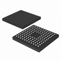
MCU 32BIT 64KB FLASH 112-BGA
Manufacturer
Energy Micro
Series
Geckor
Datasheets
1.EFM32-G890F128-SK.pdf
(70 pages)
2.EFM32-G890F128-SK.pdf
(10 pages)
3.EFM32G200F16.pdf
(463 pages)
4.EFM32G200F16.pdf
(136 pages)
Specifications of EFM32G890F64
Core Processor
ARM® Cortex-M3™
Core Size
32-Bit
Speed
32MHz
Connectivity
EBI/EMI, I²C, IrDA, SmartCard, SPI, UART/USART
Peripherals
Brown-out Detect/Reset, DMA, LCD, POR, PWM, WDT
Number Of I /o
90
Program Memory Size
64KB (64K x 8)
Program Memory Type
FLASH
Ram Size
16K x 8
Voltage - Supply (vcc/vdd)
1.8 V ~ 3.8 V
Data Converters
A/D 8x12b, D/A 2x12b
Oscillator Type
External
Operating Temperature
-40°C ~ 85°C
Package / Case
112-LFBGA
Processor Series
EFM32G890
Core
ARM Cortex-M3
Data Bus Width
32 bit
Data Ram Size
16 KB
Interface Type
I2C, UART
Maximum Clock Frequency
32 MHz
Number Of Programmable I/os
90
Number Of Timers
3
Operating Supply Voltage
1.8 V to 3.8 V
Maximum Operating Temperature
+ 85 C
Mounting Style
SMD/SMT
Minimum Operating Temperature
- 40 C
Lead Free Status / RoHS Status
Lead free / RoHS Compliant
Eeprom Size
-
Lead Free Status / Rohs Status
Details
Available stocks
Company
Part Number
Manufacturer
Quantity
Price


4.2 Alternate functionality pinout
2010-12-17 - d0010_Rev1.20
A wide selection of alternate functionality is available for multiplexing to various pins. This is shown in
Table 4.2 (p. 52) . The table shows the name of the alternate functionality in the first column, followed
by columns showing the possible LOCATION bitfield settings.
Note
Table 4.2. Alternate functionality overview
Alternate
Functionality
ACMP0_CH0
ACMP0_CH1
ACMP0_CH2
ACMP0_CH3
ACMP0_CH4
ACMP0_CH5
ACMP0_CH6
ACMP0_CH7
ACMP0_O
ACMP1_CH0
ACMP1_CH1
ACMP1_CH2
ACMP1_CH3
ACMP1_CH4
ACMP1_CH5
ACMP1_CH6
ACMP1_CH7
ACMP1_O
ADC0_CH0
ADC0_CH1
ADC0_CH2
ADC0_CH3
ADC0_CH4
ADC0_CH5
ADC0_CH6
ADC0_CH7
CMU_CLK0
CMU_CLK1
DAC0_OUT0
DAC0_OUT1
DBG_SWCLK
Some functionality, such as analog interfaces, do not have alternate settings or a LOCA-
TION bitfield. In these cases, the pinout is shown in the column corresponding to LOCA-
TION 0.
PC0
PC1
PC2
PC3
PC4
PC5
PC6
PC7
PE13
PC8
PC9
PC10
PC11
PC12
PC13
PC14
PC15
PF2
PD0
PD1
PD2
PD3
PD4
PD5
PD6
PD7
PA2
PA1
PB11
PB12
PF0
0
PE2
PE3
PC12
PD8
PF0
LOCATION
1
2
3
...the world's most energy friendly microcontrollers
52
Analog comparator ACMP0, channel 0.
Analog comparator ACMP0, channel 1.
Analog comparator ACMP0, channel 2.
Analog comparator ACMP0, channel 3.
Analog comparator ACMP0, channel 4.
Analog comparator ACMP0, channel 5.
Analog comparator ACMP0, channel 6.
Analog comparator ACMP0, channel 7.
Analog comparator ACMP0, digital output.
Analog comparator ACMP1, channel 0.
Analog comparator ACMP1, channel 1.
Analog comparator ACMP1, channel 2.
Analog comparator ACMP1, channel 3.
Analog comparator ACMP1, channel 4.
Analog comparator ACMP1, channel 5.
Analog comparator ACMP1, channel 6.
Analog comparator ACMP1, channel 7.
Analog comparator ACMP1, digital output.
Analog to digital converter ADC0, input channel number 0.
Analog to digital converter ADC0, input channel number 1.
Analog to digital converter ADC0, input channel number 2.
Analog to digital converter ADC0, input channel number 3.
Analog to digital converter ADC0, input channel number 4.
Analog to digital converter ADC0, input channel number 5.
Analog to digital converter ADC0, input channel number 6.
Analog to digital converter ADC0, input channel number 7.
Clock Management Unit, clock output number 0.
Clock Management Unit, clock output number 1.
Digital to Analog Converter DAC0 output channel number 0.
Digital to Analog Converter DAC0 output channel number 1.
Debug-interface Serial Wire clock input.
Description
www.energymicro.com
Related parts for EFM32G890F64
Image
Part Number
Description
Manufacturer
Datasheet
Request
R

Part Number:
Description:
KIT STARTER EFM32 GECKO
Manufacturer:
Energy Micro
Datasheet:

Part Number:
Description:
KIT DEV EFM32 GECKO LCD SUPPORT
Manufacturer:
Energy Micro
Datasheet:

Part Number:
Description:
BOARD PROTOTYPING FOR EFM32
Manufacturer:
Energy Micro
Datasheet:

Part Number:
Description:
KIT DEVELOPMENT EFM32 GECKO
Manufacturer:
Energy Micro
Datasheet:

Part Number:
Description:
MCU, MPU & DSP Development Tools TG840 Sample Kit
Manufacturer:
Energy Micro
Datasheet:

Part Number:
Description:
MCU, MPU & DSP Development Tools TG Starter Kit
Manufacturer:
Energy Micro
Datasheet:
Part Number:
Description:
MCU, MPU & DSP Development Tools TG108 Sample Kit
Manufacturer:
Energy Micro
Part Number:
Description:
MCU, MPU & DSP Development Tools TG210 Sample Kit
Manufacturer:
Energy Micro
Datasheet:
Part Number:
Description:
MCU, MPU & DSP Development Tools TG822 Sample Kit
Manufacturer:
Energy Micro
Datasheet:
Part Number:
Description:
MCU, MPU & DSP Development Tools TG230 Sample Kit
Manufacturer:
Energy Micro

Part Number:
Description:
SAMPLE KIT (SMALL BOX - CONTAINING 2 DEVICES)
Manufacturer:
Energy Micro
Part Number:
Description:
SAMPLE KIT (SMALL BOX - CONTAINING 2 DEVICES)
Manufacturer:
Energy Micro