EFM32G890F64 Energy Micro, EFM32G890F64 Datasheet - Page 67
EFM32G890F64
Manufacturer Part Number
EFM32G890F64
Description
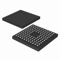
MCU 32BIT 64KB FLASH 112-BGA
Manufacturer
Energy Micro
Series
Geckor
Datasheets
1.EFM32-G890F128-SK.pdf
(70 pages)
2.EFM32-G890F128-SK.pdf
(10 pages)
3.EFM32G200F16.pdf
(463 pages)
4.EFM32G200F16.pdf
(136 pages)
Specifications of EFM32G890F64
Core Processor
ARM® Cortex-M3™
Core Size
32-Bit
Speed
32MHz
Connectivity
EBI/EMI, I²C, IrDA, SmartCard, SPI, UART/USART
Peripherals
Brown-out Detect/Reset, DMA, LCD, POR, PWM, WDT
Number Of I /o
90
Program Memory Size
64KB (64K x 8)
Program Memory Type
FLASH
Ram Size
16K x 8
Voltage - Supply (vcc/vdd)
1.8 V ~ 3.8 V
Data Converters
A/D 8x12b, D/A 2x12b
Oscillator Type
External
Operating Temperature
-40°C ~ 85°C
Package / Case
112-LFBGA
Processor Series
EFM32G890
Core
ARM Cortex-M3
Data Bus Width
32 bit
Data Ram Size
16 KB
Interface Type
I2C, UART
Maximum Clock Frequency
32 MHz
Number Of Programmable I/os
90
Number Of Timers
3
Operating Supply Voltage
1.8 V to 3.8 V
Maximum Operating Temperature
+ 85 C
Mounting Style
SMD/SMT
Minimum Operating Temperature
- 40 C
Lead Free Status / RoHS Status
Lead free / RoHS Compliant
Eeprom Size
-
Lead Free Status / Rohs Status
Details
Available stocks
Company
Part Number
Manufacturer
Quantity
Price


...the world's most energy friendly microcontrollers
List of Figures
1.1. Block Diagram ....................................................................................................................................... 2
2.1. EFM32G890 Memory Map with largest RAM and Flash sizes .......................................................................... 8
3.1. EM0 Current consumption while executing prime number calculation code from flash with HFRCO running at
28MHz ..................................................................................................................................................... 12
3.2. EM0 Current consumption while executing prime number calculation code from flash with HFRCO running at
21MHz ..................................................................................................................................................... 12
3.3. EM0 Current consumption while executing prime number calculation code from flash with HFRCO running at
14MHz ..................................................................................................................................................... 13
3.4. EM0 Current consumption while executing prime number calculation code from flash with HFRCO running at
11MHz ..................................................................................................................................................... 13
3.5. EM0 Current consumption while executing prime number calculation code from flash with HFRCO running at
7MHz ....................................................................................................................................................... 14
3.6. EM1 Current consumption with all peripheral clocks disabled and HFRCO running at 28MHz ............................... 14
3.7. EM1 Current consumption with all peripheral clocks disabled and HFRCO running at 21MHz ............................... 15
3.8. EM1 Current consumption with all peripheral clocks disabled and HFRCO running at 14MHz ............................... 15
3.9. EM1 Current consumption with all peripheral clocks disabled and HFRCO running at 11MHz ............................... 16
3.10. EM1 Current consumption with all peripheral clocks disabled and HFRCO running at 7MHz ............................... 16
3.11. EM2 current consumption. RTC prescaled to 1kHz, 32 kHz LFRCO. ............................................................. 17
3.12. EM3 current consumption. ................................................................................................................... 17
3.13. EM4 current consumption. ................................................................................................................... 18
3.14. Typical Low-Level Output Current, 2V Supply Voltage ................................................................................ 21
3.15. Typical High-Level Output Current, 2V Supply Voltage ................................................................................ 22
3.16. Typical Low-Level Output Current, 3V Supply Voltage ................................................................................ 23
3.17. Typical High-Level Output Current, 3V Supply Voltage ................................................................................ 24
3.18. Typical Low-Level Output Current, 3.8V Supply Voltage .............................................................................. 25
3.19. Typical High-Level Output Current, 3.8V Supply Voltage ............................................................................. 26
3.20. Calibrated LFRCO Frequency vs Temperature and Supply Voltage .............................................................. 28
3.21. Calibrated HFRCO 1 MHz Band Frequency vs Temperature and Supply Voltage ............................................ 30
3.22. Calibrated HFRCO 7 MHz Band Frequency vs Temperature and Supply Voltage ............................................ 30
3.23. Calibrated HFRCO 11 MHz Band Frequency vs Temperature and Supply Voltage ........................................... 30
3.24. Calibrated HFRCO 14 MHz Band Frequency vs Temperature and Supply Voltage ........................................... 31
3.25. Calibrated HFRCO 21 MHz Band Frequency vs Temperature and Supply Voltage ........................................... 31
3.26. Calibrated HFRCO 28 MHz Band Frequency vs Temperature and Supply Voltage ........................................... 31
3.27. Integral Non-Linearity (INL) ................................................................................................................... 36
3.28. Differential Non-Linearity (DNL) .............................................................................................................. 36
3.29. ADC Frequency Spectrum, Vdd = 3V, Temp = 25° ................................................................................... 37
3.30. ADC Integral Linearity Error vs Code, Vdd = 3V, Temp = 25° ..................................................................... 38
3.31. ADC Differental Linearity Error vs Code, Vdd = 3V, Temp = 25° .................................................................. 39
3.32. ADC Absolute Offset, Common Mode = Vdd /2 ........................................................................................ 40
3.33. ADC Dynamic Performance vs Temperature for all ADC References, Vdd = 3V .............................................. 40
3.34. ADC Temperature sensor readout ......................................................................................................... 41
3.35. Typical ACMP Characteristics ............................................................................................................... 44
4.1. EFM32G890 Pinout (top view, not to scale) ............................................................................................... 48
4.2. BGA112 .............................................................................................................................................. 56
5.1. BGA112 PCB Land Pattern ..................................................................................................................... 58
5.2. BGA112 PCB Solder Mask ..................................................................................................................... 58
5.3. BGA112 PCB Stencil Design ................................................................................................................... 59
6.1. Example Chip Marking ........................................................................................................................... 60
www.energymicro.com
2010-12-17 - d0010_Rev1.20
67
Related parts for EFM32G890F64
Image
Part Number
Description
Manufacturer
Datasheet
Request
R

Part Number:
Description:
KIT STARTER EFM32 GECKO
Manufacturer:
Energy Micro
Datasheet:

Part Number:
Description:
KIT DEV EFM32 GECKO LCD SUPPORT
Manufacturer:
Energy Micro
Datasheet:

Part Number:
Description:
BOARD PROTOTYPING FOR EFM32
Manufacturer:
Energy Micro
Datasheet:

Part Number:
Description:
KIT DEVELOPMENT EFM32 GECKO
Manufacturer:
Energy Micro
Datasheet:

Part Number:
Description:
MCU, MPU & DSP Development Tools TG840 Sample Kit
Manufacturer:
Energy Micro
Datasheet:

Part Number:
Description:
MCU, MPU & DSP Development Tools TG Starter Kit
Manufacturer:
Energy Micro
Datasheet:
Part Number:
Description:
MCU, MPU & DSP Development Tools TG108 Sample Kit
Manufacturer:
Energy Micro
Part Number:
Description:
MCU, MPU & DSP Development Tools TG210 Sample Kit
Manufacturer:
Energy Micro
Datasheet:
Part Number:
Description:
MCU, MPU & DSP Development Tools TG822 Sample Kit
Manufacturer:
Energy Micro
Datasheet:
Part Number:
Description:
MCU, MPU & DSP Development Tools TG230 Sample Kit
Manufacturer:
Energy Micro

Part Number:
Description:
SAMPLE KIT (SMALL BOX - CONTAINING 2 DEVICES)
Manufacturer:
Energy Micro
Part Number:
Description:
SAMPLE KIT (SMALL BOX - CONTAINING 2 DEVICES)
Manufacturer:
Energy Micro