TFA9879HN/N1,157 NXP Semiconductors, TFA9879HN/N1,157 Datasheet
TFA9879HN/N1,157
Specifications of TFA9879HN/N1,157


Related parts for TFA9879HN/N1,157


TFA9879HN/N1,157 Summary of contents
Page 1
TFA9879 Mono BTL class-D audio amplifier for portable applications with digital input Rev. 02 — 15 October 2010 1. Introduction The TFA9879 is a high-efficiency filter-free mono class-D audio amplifier with two separate digital inputs for mobile applications. 2. General ...
Page 2
... NXP Semiconductors 1 3.3 V tolerant digital inputs Only three external components required 3.2 Programmable Digital Sound Processor (DSP) Digital volume control (− +24 dB) Digital parametric 5-band equalizer Bass and treble control (− +18 dB) Dynamic range compressor: Programmable attack and release levels Programmable attack and release rates ...
Page 3
... NXP Semiconductors 5. Quick reference data Table 1. Quick reference data All parameters are guaranteed for V ° unless otherwise specified. amb Symbol Parameter V power supply voltage DDP V digital supply voltage DDD I supply current P I digital supply current DDD P RMS output power o(RMS) η ...
Page 4
... NXP Semiconductors 7. Block diagram V DDD 23 SDA SCL 2 CONTROL TFA9879 SDI1 20 21 SCK1 22 LRCK1 MUX SDI2 17 RECEIVER SCK2 18 LRCK2 19 HIGH VOLUME PASS CONTROL FILTER DRC DSP ADSEL1 16 ADSEL2 4 24 GNDD Fig 1. Block diagram TFA9879 Product data sheet Mono BTL class-D audio amplifier with digital input n ...
Page 5
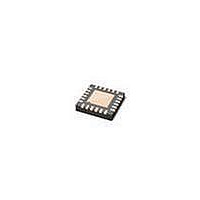
... NXP Semiconductors 8. Pinning information 8.1 Pinning (1) Exposed Die Attach Paddle (DAP) Fig 2. 8.2 Pin description Table 3. Symbol SDA SCL TEST1 ADSEL2 TEST3 n.c. V DDP OUTB OUTA GNDP STABA n.c TEST2 ADSEL1 SDI2 SCK2 LRCK2 SDI1 SCK1 LRCK1 TFA9879 Product data sheet ...
Page 6
... NXP Semiconductors Table 3. Symbol V DDD GNDD DAP 9. Functional description The TFA9879 is a high-efficiency mono Bridge Tied Load (BTL) class-D amplifier with digital audio inputs. It supports all commonly used formats. The key functional blocks of the TFA9879 are shown in audio signal is processed and converted into a Pulse Width Modulated (PWM) signal using a 3-level modulation ...
Page 7
... NXP Semiconductors The following protection circuits are built into the TFA9879: • OverTemperature Protection (OTP) • OverCurrent Protection (OCP) • UnderFrequency Protection (UFP) • OverFrequency Protection (OFP) • Invalid Bit-clock Protection (IBP) • DC-blocking 9.1 Operating modes The TFA9879 supports the following operating modes, which are controlled via the ...
Page 8
... NXP Semiconductors Fig 3. 9.1.2 Supported Digital audio data formats The TFA9879 supports a commonly used range of I formats. The I (Table 22), are listed in TFA9879 automatically detects the number of slots by measuring the ratio between the sync frequency (8 kHz) and the data clock. PCM/IOM2 formats. ...
Page 9
... NXP Semiconductors Table 4. SCK frequency LEFT BCK DATA MSB B2 WS LEFT BCK DATA MSB B2 WS LEFT BCK DATA WS LEFT BCK DATA WS LEFT 20 BCK DATA MSB WS LEFT BCK DATA MSB Fig 4. I S-supported digital audio data formats TFA9879 Product data sheet Mono BTL class-D audio amplifier with digital input ...
Page 10
... NXP Semiconductors Table 5. Number of slots reserved LRCK SCK SDI MSB B2 Slot 0 LRCK SCK SDI MSB B2 Slot 0 Fig 5. PCM/IOM2-supported digital audio data formats TFA9879 Product data sheet Mono BTL class-D audio amplifier with digital input PCM/IOM2-supported audio data formats f (kHz) Sync frequency ...
Page 11
... NXP Semiconductors 9.2 Digital Signal Processor (DSP) features 9.2.1 Serial interface selection The TFA9879 contains two serial interfaces. The active interface is selected via bit INPUT_SEL in the Device control register (see following sequence is initiated: • Soft mute is activated for 128/f • The TFA9879 switches to Off mode and the serial interface input is toggled • ...
Page 12
... NXP Semiconductors The de-emphasis filter is a simple first order filter. The cut-off frequency of the de-emphasis low-pass filter is approximately 3.5 kHz. The TFA9879 de-emphasis filter is supported for four sample frequencies, as detailed in Table 6. [1:0] Control value [ [1] Value selected via bits DE_PHAS in the De-emphasis, soft/hard mute and power limiter control register ...
Page 13
... NXP Semiconductors Fig 6. The transfer function of this all-pass filter is given A(z) is the second order filter structure. The transfer function of A(z) is given in Equation −1 Z equals one and Equation Equation The ranges of the parametric equalizer settings for each band are: The gain from − +12 dB. ...
Page 14
... NXP Semiconductors For optimum numerical noise performance, different configurations are available for a given filter transfer function. The binary filter configuration parameters t actual configuration and should be chosen according to ⎛ 0 ⎜ ⎝ ⎛ 0 ⎜ ⎝ A maximum amplification, with respect to the input signal, can be achieved per equalizer stage ...
Page 15
... NXP Semiconductors Table 8. Word word1 word1 word1 word2 word2 word2 word2 word2 Fig 7. (dB) Fig 8. TFA9879 Product data sheet Mono BTL class-D audio amplifier with digital input Equalizer control word construction Section Data [14:4] 11 mantissa bits of k [3:0] four exponent bits of k ...
Page 16
... NXP Semiconductors (dB) Fig 9. 9.2.6 Bass and treble control The TFA9879 contains first order shelving filters for bass and treble control. The device can attenuate or boost the bass and high frequency signals independently steps within a − +18 dB range. Attenuation and boosting are dependent on the audio signal zero crossing settings (see corner frequencies are adjustable ...
Page 17
... NXP Semiconductors Figure 10 sample rate of 48 kHz and a corner frequency of 272 Hz. Fig 10. Bass function steps; the treble control is set to flat Figure 11 sample rate of 48 kHz and a corner frequency of 1630 Hz. Fig 11. Treble function steps; the bass control is set to flat 9.2.7 Muting The TFA9879 support two muting options, which are controlled via the I • ...
Page 18
... NXP Semiconductors Soft muting prevents audible pops. The function smoothly reduces the gain setting of the audio channel to the mute level according to a raised cosine shape. Soft muting is performed in 128 / f Table 32 The hard mute function immediately switches the outputs duty-cycle pulses result, the input signals are abruptly blocked. Hard mute takes priority over soft mute. ...
Page 19
... NXP Semiconductors 9.2.10.1 Functional description The DRC compresses the dynamic range of the audio stream. The volume control, equalizer or bass/treble controls can be set so that the audio stream exceeds the 0 dBFs clip level. The DRC can be programmed to compress the louder audio content when this occurs, while quieter sounds remain unaffected, i ...
Page 20
... NXP Semiconductors audio in audio out attack level (peak value) release level (RMS-value) attack level (peak value) Fig 13. DRC attack and release behavior Table 11. Control value: attack level 0000 0001 0010 0011 0100 0101 0110 0111 1000 [4] 1001 1010 1011 1100 1101 ...
Page 21
... NXP Semiconductors Table 12. Control value: attack rate 0000 0001 [3] 0010 0011 0100 0101 0110 0111 1000 1001 1010 1011 1100 1101 1110 1111 [1] The control value is selected via bits AT_RATE in the DRC control register (see [2] The control value is selected via bits RL_RATE in the DRC control register (see [3] Default value ...
Page 22
... NXP Semiconductors The maximum peak output voltage for the first ten power limiter gain settings is given in Table 13. Table 13. All parameters are guaranteed for amb Control value [2] 00h 01h 02h 03h 04h 05h 06h 07h 08h 09h [1] The control value is selected via bits P_LIM in the De-emphasis, soft/hard mute and power limiter control ...
Page 23
... NXP Semiconductors • OverTemperature Protection (OTP) • OverCurrent Protection (OCP) • UnderFrequency Protection (UFP) • OverFrequency Protection (OFP) • Invalid Bit-clock Protection (IBP) • DC-blocking via high-pass filter (see The reaction of the device to fault conditions differs depending on the protection circuit involved. ...
Page 24
... NXP Semiconductors 9.4.4 OverFrequency Protection (OFP) OFP sets the output stages floating when the clock input source is too high (>f can happen if, for example, the selected sample frequency (bits I2S_FS in in line with the applied sample rate. The PWM controller can become unstable when the frequency of the input clock is higher than the selected sample frequency ...
Page 25
... NXP Semiconductors The TFA9879 is accessed via an 8-bit code (see address. Bit 0 (R/W) indicates whether a read ( write (0) operation has been requested. Four separate addresses are supported for multichannel applications. Applying the appropriate voltage to pins ADSEL1 (A1) and ADSEL2 (A2) select the required I Table 16. ...
Page 26
... NXP Semiconductors 2 10.3 I C-bus read cycle The sequence of events that needs to be followed when reading data from the TFA9879’ C-bus registers is detailed in registers stores two bytes of data. Data is always written in byte pairs. Data transfer is always MSB first. The read cycle sequence using SDA is as follows: 1 ...
Page 27
... NXP Semiconductors Table 20. Register address (hex) 06h 07h 08h 09h 0Ah 0Bh 0Ch 0Dh 0Eh 0Fh 10h 11h 12h 13h 14h 15h The following subsections provide details of the of the bits in these registers and the control and status functionality assigned to each. 10.4.1 Device control Table 21 ...
Page 28
... NXP Semiconductors 10.4.2 Serial interface control Table 22. Bit 15:12 reserved 11:10 MONO_SEL 9:6 5:3 2 TFA9879 Product data sheet Mono BTL class-D audio amplifier with digital input Serial interface control registers (addresses 01h and 03h Symbol Access Default 0000 R/W 10 I2S_FS R/W ...
Page 29
... NXP Semiconductors Table 22. Bit 1:0 [1] Serial interface 1 settings are controlled via register 01h; serial interface 2 settings are controlled via register 03h. Table 23. Bit 15:12 reserved 7:4 3:0 [1] PCM/IOM2 format settings of serial interface 1 are controlled via register 02h; PCM/IOM2 format settings of serial interface 2 are controlled via register 04h. ...
Page 30
... NXP Semiconductors 10.4.3 Equalizer configuration Table 24. ‘x’ represents the equalizer band Bit 15 14:4 3:0 [1] Default settings are given in Table 25. ‘x’ represents the equalizer band Bit 15 14:11 EQx_k2m 10:8 7:1 0 [1] Default settings are given in Table 26. Band Frequency (Hz) 100 Q-factor ...
Page 31
... NXP Semiconductors 10.4.4 Bypass control Table 27. Bit 15:8 7:6 5 10.4.5 Dynamic range compressor Table 28. Bit 15:12 AT_LVL 11:8 37:4 3:0 TFA9879 Product data sheet Mono BTL class-D audio amplifier with digital input Bypass control register (addresses 0Fh) bit description Symbol Access ...
Page 32
... NXP Semiconductors 10.4.6 Bass and treble control Table 29. Bit 15:14 reserved 13:9 8:7 6:2 1:0 10.4.7 High-pass filter Table 30. Bit 15:9 8:0 [1] Default value is 04h. From TFA9879 Product data sheet Mono BTL class-D audio amplifier with digital input Bass and treble control register (addresses 11h) bit description ...
Page 33
... NXP Semiconductors 10.4.8 Volume control Table 31. Bit 15:13 reserved 12 11:8 7:0 10.4.9 De-emphasis, soft/hard mute and power limiter Table 32. Bit 15:12 reserved 11:10 DE_PHAS 9 8 7:0 TFA9879 Product data sheet Mono BTL class-D audio amplifier with digital input Volume control register (address 13h) bit description ...
Page 34
... NXP Semiconductors 10.4.10 Miscellaneous status Table 33. Bit 12:11 reserved 10 TFA9879 Product data sheet Mono BTL class-D audio amplifier with digital input Miscellaneous status register (address 15h) bit description Symbol Access Description reserved PS R power stage status: 0: class-D audio amplifier power stage floating 1: class-D audio amplifier power stage switching ...
Page 35
... NXP Semiconductors Table 33. Bit TFA9879 Product data sheet Mono BTL class-D audio amplifier with digital input Miscellaneous status register (address 15h) bit description Symbol Access Description UFP(1) R underfrequency protection on serial interface input 1: 0: the frequency of the signal on pin LRCK1 is in line with (or ...
Page 36
... NXP Semiconductors 11. Internal circuitry Table 34. Internal circuitry Pin Symbol 1 SDA 2 SCL 3 TEST1 4 ADSEL2 5 TEST3 16 ADSEL1 17 SDI2 18 SCK2 19 LRCK2 20 SDI1 21 SCK1 22 LRCK2 7,8 V DDP TFA9879 Product data sheet Mono BTL class-D audio amplifier with digital input Equivalent circuit 1 11, 12 11, 12 11, 12, 24 All information provided in this document is subject to legal disclaimers. Rev. 02 — ...
Page 37
... NXP Semiconductors Table 34. Internal circuitry Pin Symbol 9 OUTB 10 OUTA 13 STABA 15 TEST2 12. Limiting values Table 35. Limiting values In accordance with the Absolute Maximum Rating System (IEC 60134). Symbol Parameter V analog supply voltage DDA V digital supply voltage DDD T junction temperature j T storage temperature stg ...
Page 38
... NXP Semiconductors 13. Thermal characteristics Table 36. Thermal characteristics Symbol Parameter R thermal resistance from junction to ambient th(j-a) Ψ thermal characterization parameter from j-lead junction to lead Ψ thermal characterization parameter from j-top junction to top of package R thermal resistance from junction to case th(j-c) [1] Measured on a JEDEC high K-factor test board (standard EIA/JESD 51-7). ...
Page 39
... NXP Semiconductors 14. Characteristics 14.1 DC Characteristics Table 37. DC characteristics All parameters are guaranteed for V ° unless otherwise specified. amb Symbol Parameter V power supply voltage DDP V digital supply voltage DDD I supply current P I digital supply current DDD Series resistance output power switches R drain-source on-state resistance DSon Amplifier output pins ...
Page 40
... NXP Semiconductors 14.2 AC characteristics Table 38. AC characteristics All parameters are guaranteed for V ° unless otherwise specified. amb Symbol Parameter Class D amplifier P RMS output power o(RMS) η output power efficiency po THD+N total harmonic distortion-plus-noise P V output noise voltage n(o) S/N signal-to-noise ratio ...
Page 41
... NXP Semiconductors 2 14 timing characteristics 2 Table 39. I C-bus interface characteristics; see All parameters are guaranteed for V unless otherwise specified. Symbol Parameter f SCL clock frequency SCL t LOW period of the SCL clock LOW t HIGH period of the SCL clock HIGH t rise time r t fall time ...
Page 42
... NXP Semiconductors 2 14 timing characteristics 2 Table 40 bus interface characteristics; see All parameters are guaranteed for V ° unless otherwise specified. amb Symbol Parameter f sampling frequency s f clock frequency clk t set-up time su t hold time h [ load resistance load inductance Fig 15. I TFA9879 Product data sheet ...
Page 43
... NXP Semiconductors 14.5 PCM/IOM2 timing characteristics Table 41. PCM/IOM2 characteristics; see All parameters are guaranteed for V ° unless otherwise specified. amb Symbol Parameter f pulse frequency p f clock frequency clk t set-up time su t hold time h t pulse duration p [ load resistance load inductance SCK ...
Page 44
... NXP Semiconductors 15. Application information The TFA9879 is a filter-free BTL class-D amplifier that uses a fixed frequency PWM modulation scheme (see the simplified application schematic in TFA9879 is idle (no audio input signal), the voltage across the speaker generating no additional current. Even when the PWM output is modulated by the audio input signal, the out-of-band AC ripple current in the voice coil is very small compared to the audio current ...
Page 45
... NXP Semiconductors 15.1.2 Output current limiting The peak output current I level is 1.3 A. During normal operation, the output current should not exceed this threshold level, otherwise the audio signal will be distorted. The peak output current in BTL configuration can be calculated using max where: ...
Page 46
... NXP Semiconductors 15.4 PCB layout considerations Great care should be taken when designing the PCB layout for a Class-D amplifier circuit as the layout can affect the audio performance, the EMC performance and/or the thermal performance, and can even affect the functionality of the TFA9879. ...
Page 47
... NXP Semiconductors 15.5 Typical application diagram (simplified) BASEBAND PROCESSOR output output MULTIMEDIA PROCESSOR address select 1 address select 2 Fig 18. Typical application (simplified) TFA9879 Product data sheet Mono BTL class-D audio amplifier with digital input LRCK1 22 SCK1 21 SDI1 20 LRCK2 19 TFA8979HN SCK2 18 SDI2 17 SCL ...
Page 48
... NXP Semiconductors 15.6 Curves measured in reference design (demonstration board) All measurements were taken with V high-pass filter off, unless otherwise specified THD+N (%) 10 1 −1 10 (1) (3) −2 10 (2) −3 10 −2 − ( kHz kHz 100 Hz Ω 3 DDP THD+N (%) 10 1 −1 10 (1) (2) (3) −2 10 −3 10 − ...
Page 49
... NXP Semiconductors 2 10 THD+N (%) 10 1 −1 10 (2) −2 (1) 10 − ( 100 500 Ω 3 DDP THD+N (%) 10 1 −1 10 (1) −2 10 (2) − ( 100 500 Ω 3 DDP L Fig 20. Total harmonic distortion-plus-noise as a function of frequency TFA9879 Product data sheet Mono BTL class-D audio amplifier with digital input ...
Page 50
... NXP Semiconductors 2 10 THD+N (%) 10 1 −1 10 −2 10 − ( Hz) ripple ripple ( 217 Hz ripple ( kHz ripple ( kHz ripple = 8 Ω 3 DDP 200 mV (RMS) ripple Fig 21. Total harmonic distortion-plus-noise and power supply intermodulation distortion as a function of frequency (1) 0 (2) (3) −10 −20 −30 − Ω 3 DDP ...
Page 51
... NXP Semiconductors (1) A-weighted (2) 20 kHz brickwall filter Fig 24. Signal-to-noise ratio as a function of output power ( Ω (1) THD Ω (2) THD Ω (3) THD Ω (4) THD 100 Hz, clip control on i Fig 25. Output power as a function of supply voltage TFA9879 Product data sheet Mono BTL class-D audio amplifier with digital input ...
Page 52
... NXP Semiconductors 0.20 P (W) 0.15 0.10 0.05 (2) (1) 0.00 −3 −2 − ( 3.7 V DDP ( DDP = 8 Ω kHz, clip control off L i Fig 26. Power dissipation as a function of output power 100 (1) η (%) ( 0 3.7 V DDP ( DDP = 8 Ω kHz, clip control off L i Fig 27. Efficiency as a function of output power ...
Page 53
... NXP Semiconductors 16. Package outline HVQFN24: plastic thermal enhanced very thin quad flat package; no leads; 24 terminals; body 0.85 mm terminal 1 index area terminal 1 24 index area DIMENSIONS (mm are the original dimensions) (1) A UNIT max. 0.05 0. 0.2 0.00 0.18 Note 1. Plastic or metal protrusions of 0.075 mm maximum per side are not included. ...
Page 54
... NXP Semiconductors 17. Soldering of SMD packages This text provides a very brief insight into a complex technology. A more in-depth account of soldering ICs can be found in Application Note AN10365 “Surface mount reflow soldering description”. 17.1 Introduction to soldering Soldering is one of the most common methods through which packages are attached to Printed Circuit Boards (PCBs), to form electrical circuits ...
Page 55
... NXP Semiconductors 17.4 Reflow soldering Key characteristics in reflow soldering are: • Lead-free versus SnPb soldering; note that a lead-free reflow process usually leads to higher minimum peak temperatures (see reducing the process window • Solder paste printing issues including smearing, release, and adjusting the process window for a mix of large and small components on one board • ...
Page 56
... NXP Semiconductors Fig 29. Temperature profiles for large and small components For further information on temperature profiles, refer to Application Note AN10365 “Surface mount reflow soldering description”. TFA9879 Product data sheet Mono BTL class-D audio amplifier with digital input maximum peak temperature = MSL limit, damage level ...
Page 57
... NXP Semiconductors 18. Revision history Table 44. Revision history Document ID Release date TFA9879 v.2 20101015 • Modifications: Specification status changed to Product data sheet TFA9879 v.1 20100408 TFA9879 Product data sheet Mono BTL class-D audio amplifier with digital input Data sheet status Product data sheet Preliminary data sheet All information provided in this document is subject to legal disclaimers ...
Page 58
... In no event shall NXP Semiconductors be liable for any indirect, incidental, punitive, special or consequential damages (including - without limitation - lost profits, lost savings, business interruption, costs related to the removal or ...
Page 59
... NXP Semiconductors’ specifications such use shall be solely at customer’s own risk, and (c) customer fully indemnifies NXP Semiconductors for any liability, damages or failed product claims resulting from customer design and use of the product for automotive applications beyond NXP Semiconductors’ ...
Page 60
... NXP Semiconductors 21. Contents 1 Introduction . . . . . . . . . . . . . . . . . . . . . . . . . . . . 1 2 General description . . . . . . . . . . . . . . . . . . . . . . 1 3 Features and benefits . . . . . . . . . . . . . . . . . . . . 1 3.1 General features . . . . . . . . . . . . . . . . . . . . . . . . 1 3.2 Programmable Digital Sound Processor (DSP) 2 3.3 Interface format support for digital audio inputs 2 4 Applications . . . . . . . . . . . . . . . . . . . . . . . . . . . . 2 5 Quick reference data . . . . . . . . . . . . . . . . . . . . . 3 6 Ordering information . . . . . . . . . . . . . . . . . . . . . 3 7 Block diagram . . . . . . . . . . . . . . . . . . . . . . . . . . 4 8 Pinning information . . . . . . . . . . . . . . . . . . . . . . 5 8 ...