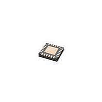
TFA9879HN/N1,157 NXP Semiconductors, TFA9879HN/N1,157 Datasheet - Page 43

TFA9879HN/N1,157
Manufacturer Part Number
TFA9879HN/N1,157
Description
IC AMP AUDIO DGTL MONO D 24HVQFN
Manufacturer
NXP Semiconductors
Type
Class Dr
Datasheet
1.TFA9879HNN1118.pdf
(60 pages)
Specifications of TFA9879HN/N1,157
Output Type
1-Channel (Mono)
Package / Case
24-VFQFN Exposed Pad
Max Output Power X Channels @ Load
2.75W x 1 @ 4 Ohm
Voltage - Supply
2.5 V ~ 5.5 V
Features
Depop, Digital Inputs, I²C, I²S, Mute, Short-Circuit and Thermal Protection, Tone and Volume Control
Mounting Type
Surface Mount
Product
Class-D
Output Power
2.75 W
Thd Plus Noise
0.02 %
Operating Supply Voltage
3.7 V
Supply Current
5.7 mA
Mounting Style
SMD/SMT
Audio - Load Impedance
4 Ohms, 8 Ohms
Audio Load Resistance
4 Ohms, 8 Ohms
Input Signal Type
Serial
Supply Voltage (max)
5.5 V
Supply Voltage (min)
2.5 V
Lead Free Status / RoHS Status
Lead free / RoHS Compliant
NXP Semiconductors
Table 41.
All parameters are guaranteed for V
T
[1]
TFA9879
Product data sheet
Symbol
f
f
t
t
t
p
clk
su
h
p
amb
Fig 16. PCM/IOM2 timing
R
= 25
L
= load resistance; L
°
C unless otherwise specified.
PCM/IOM2 characteristics; see
SCK
LRCK, FSC (long)
LRCK, FSC (short)
SDI
Parameter
pulse frequency
clock frequency
set-up time
hold time
pulse duration
14.5 PCM/IOM2 timing characteristics
L
= load inductance.
DDD
= 1.8 V; V
All information provided in this document is subject to legal disclaimers.
Figure 16
Conditions
on LRCK1 or LRCK2 pins
on SCK1 or SCK2 pin
SCK HIGH to LRCK edge
SCK HIGH to SDI edge
LRCK edge to SCK HIGH
SDI edge to SCK HIGH
pulse on LRCK1 pin or LRCK2 pin
Rev. 02 — 15 October 2010
t
p
DDP
= 3.7 V, R
t
h
Mono BTL class-D audio amplifier with digital input
L
t
su
= 8
Ω
[1]
, L
L
= 44
μ
H
[1]
; f
-
16f
10
1/f
Min
10
10
10
i
= 1 kHz; clip control off;
clk
p
Typ
-
-
-
-
-
-
-
TFA9879
© NXP B.V. 2010. All rights reserved.
010aaa625
Max
8
192f
-
-
-
-
-
p
Unit
kHz
Hz
ns
ns
ns
ns
s
43 of 60


