APDS-9702-020 Avago Technologies US Inc., APDS-9702-020 Datasheet
APDS-9702-020
Specifications of APDS-9702-020
Available stocks


Related parts for APDS-9702-020


APDS-9702-020 Summary of contents
Page 1
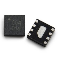
... The device is packaged in 8-pin QFN package measuring 0.55mm(H) x 2mm(W) x 2mm(L). Ordering Information Part Number Packaging APDS-9702-020 Tape & Reel Application Support Information The Application Engineering Group is available to assist you with the application design associated with APDS-9702 module. You can contact them through your local sales representatives for additional details ...
Page 2
... APDS-9702 Block Diagram (1) SDA I2C (2) SCL Oscillator Latch (3) DOUT Figure 1. APDS-9702 Block Diagram 2 ( (7) LEDA Timing Control Sunlight Cancellation (5) PD TIA PIN (6) PFILT V-I Converter + Comparator 100k 300k 500k (4) GND R1 Avago Proximity Sensor LED R3 CX3 (Optional) ...
Page 3
... APDS-9702 pin-out and I/O Configurations PIN #1 CORNER Pin 1 Pin 2 Pin 3 Pin 4 I/O Pins Configuration Table Pin Symbol Type 1 SDA Digital I/O 2 SCL Digital I/P 3 DOUT Digital O/P 4 GND Ground 5 PD Analog I/P 6 PFILT Analog O/P 7 LEDA Analog O/P 8 VCC ...
Page 4
Electrical & Optical Specifications (Ta=25°C) Parameters Symbol Input Logic High Input Voltage V IH Logic Low Input Voltage V IL Logic High Input Current I IH Logic Low Input Current I IL Shutdown Current I SD Standby Current I SB ...
Page 5
... Typical Application Circuit Rp Rp SDA SCL MCU GPIO (Optional) ADC Figure 2. Typical Application Circuit for APDS-9702 Recommended Avago Proximity Sensor Description HSDL-9100 Integrated Reflective Proximity Sensor Component Recommended Values ( with HSDL-9100 ± 5%, 0.25W R1 R2 10k: ± 1M: ± 10k: ± 5% CX1 100 nF ± 20% X 7R, Ceramic, 6.8 PF ± ...
Page 6
... I C Definition APDS-9702 operates as slave device on I described below, for more details and specifications, please refer to I SDA SCL S START condition START and STOP conditions SDA MSB SCL START or repeated START byte complete, condition interrupt within slave SDA SCL 1 START ADDRESS ...
Page 7
Register Definition Bit TRG PWR NB3 NB2 Default Register Type Description TRG Trigger This pin is active high. TRG = 1 o Normal proximity sensing operations TRG = operation ...
Page 8
Transmit Burst Pulses Definition Operation ON/OFF condition is shown in the following table: TRG PWR Condition X 0 Shut down 0 1 Standby Mode 1 1 Active Mode, pulses sent The burst pulses at LEDA pin will be activated under ...
Page 9
Output Waveforms Definition Burst Pulses LEDA V TH PFILT Object detected DOUT Figure 4. Output Waveforms Definition 9 Object detected Object not detected No object detected ...
Page 10
R Definition FILT There are built-in resistors at PFILT (pin 6) to provide 4 options to set the desired resistor for integrated RC circuit Resistor Value 0 0 Open. External resistor R3 is required parallel ...
Page 11
... APDS 9702 Performance Charts RELATIVE LED CURRENT VS VCC 1.60 1.40 1.20 1.00 0.80 0.60 0.40 0.20 0.00 2.2 2.4 2.6 2.8 3 VCC (V) RELATIVE ICC STANDY CURRENT VS VCC 1.2 1 0.8 0.6 0.4 0.2 0 2.2 2.4 2.6 2.8 3 VCC (V) AVERAGE PEAK LED CURRENT VS R1 ...
Page 12
... APDS-9702 Package Dimensions QFN 8-Pin Package Pin # Top 1 2 TOP VIEW SIDE VIEW 1.20 0. 0.125 (x4) 0.25 (x8) 0.25 (x6) BOTTOM VIEW Note: 1. All Dimensions in mm. Tolerance ±0.1mm unless specified. 2. Marking Information: The unit is marked ‘YWW LLa’ on the chip Year (Last digit of the year) ...
Page 13
Recommended Minimum Land pattern and Keep-out Area 0.25 0.5 2 SOLDER LAND PATTERN Dimension in mm. Recommended tolerances +/-0.1mm 13 Keep-out Area Recommendations: Area of Solder Land pattern = 2.3mm x 2.1mm Module placement tolerance & keep out on each ...
Page 14
... APDS-9702 Tape and Reel Dimensions Tape Dimensions 4.00 ± 0.10 4.00 ± 0.10 + .30 8.00 .10 YWW LLa UNIT ORIENTATION IN POCKET 5° MAX 2.30 ± 0. 2.00 ± .05 Ø 1.50 + .10 Ø 1.00 + 0.25 .254 ± 0.02 0.75 ± 0.10 2.30 ± 0. ALL DIMENSIONS IN mm. ...
Page 15
... SCALE 2:1 TAPE WIDTH ØA +0.0 08MM 180 –2.0 All Dimensions in mm. Packaging All APDS-9702 options are shipped in ESD proof packaging. This part is compliant to JEDEC MSL 1. Recommended Storage Conditions Storage Temperature Time from unsealing to soldering 15 W3 (INCLUDES FLANGE DISTORTION AT OUTER EDGE) ...
Page 16
... the PC board and APDS-9702 pins are heated to a temperature of 150°C to activate the flux in the solder paste. The temperature ramp up rate, R1, is limited to 3°C per second to allow for even heating of both the PC board and APDS-9702 pins ...