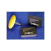
EN5364QI-E Enpirion, EN5364QI-E Datasheet - Page 4

EN5364QI-E
Manufacturer Part Number
EN5364QI-E
Description
Power Management Modules & Development Tools Eval Bd 6A Syn Buck PWM DC-DC Converter
Manufacturer
Enpirion
Type
DC/DC Switching Converters, Regulators & Controllersr
Datasheet
1.EN5364QI-E.pdf
(10 pages)
Specifications of EN5364QI-E
Input Voltage
2.375 V to 6.6 V
Output Voltage
0.6 V
Maximum Operating Temperature
+ 85 C
Minimum Operating Temperature
- 40 C
Product
Power Management Modules
For Use With/related Products
EN5364QI
Lead Free Status / RoHS Status
Lead free / RoHS Compliant
Available stocks
Company
Part Number
Manufacturer
Quantity
Price
Company:
Part Number:
EN5364QI-E
Manufacturer:
ST
Quantity:
34 000
Company:
Part Number:
EN5364QI-E
Manufacturer:
Enpirion
Quantity:
135
Figure - 1 : Output voltage programming and loop compensation. R
correspond R17 & C20 on the board. R
R13, R14, R16, or R18 on the board, depending on which jumpers are
populated on J13.
Quick Start Guide
In Figure 3, the jumper on ENA pin as shown is in disable mode. For all the J1
positions, when the jumper is between the middle and right pins the signal pin is
connected to ground or logic low. When the jumper is between the left and
middle pins, the signal pin is connected to VIN or logic High. When there is no
jumper, MAR1, MAR2 and M_S pins will be in Float mode, however ENA and
EN_PB are internally pulled low.
WARNING:
evaluation board.
STEP 1:
MAR1, MAR2, and M/S to float (no jumper).
STEP 2:
below:
VIN
AGND
Rext
SIDE
VIN
Set the “ENA” and “ENA_PB” jumper to the Disable Position. Select
Set the output voltage select jumper for the desired setting as shown
complete steps 1 through 4 before applying power to the EN53x4QI
Vf ~ 2V
IC Package
250
2.5V
Figure – 3 : J1 Mode Selection Jumpers
D1
R3
3k
EN5364QI-EN5394QI Evaluation Board Application Note
R1
100k
R2
100k
Page 4 of 10
To Gates
B
corresponds to a combination of
Figure 2: Equivalent circuit of a ternary pin
(MAR1, MAR2, or M/S) input buffer. To get a
logic High on a ternary input, pull the pin to V
through an external resistor R
populated with a 10kΩ REXT for all three ternary
pins.
November 2009 V_3
SIDE
GND
A
EXT
and C
. The board is
A
IN


