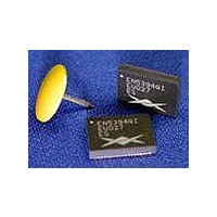
EN5364QI-E Enpirion, EN5364QI-E Datasheet - Page 5

EN5364QI-E
Manufacturer Part Number
EN5364QI-E
Description
Power Management Modules & Development Tools Eval Bd 6A Syn Buck PWM DC-DC Converter
Manufacturer
Enpirion
Type
DC/DC Switching Converters, Regulators & Controllersr
Datasheet
1.EN5364QI-E.pdf
(10 pages)
Specifications of EN5364QI-E
Input Voltage
2.375 V to 6.6 V
Output Voltage
0.6 V
Maximum Operating Temperature
+ 85 C
Minimum Operating Temperature
- 40 C
Product
Power Management Modules
For Use With/related Products
EN5364QI
Lead Free Status / RoHS Status
Lead free / RoHS Compliant
Available stocks
Company
Part Number
Manufacturer
Quantity
Price
Company:
Part Number:
EN5364QI-E
Manufacturer:
ST
Quantity:
34 000
Company:
Part Number:
EN5364QI-E
Manufacturer:
Enpirion
Quantity:
135
STEP 3:
GND (−) as indicated in Figure - 5 and set the power supply to the desired
voltage. The compensation components for the board have been optimized for
an input voltage of 5V (see Figures 1 & 7). To optimize the board for another
input voltage, calculate new values R
1. The caption in Figure 1, states which components on the PCB correspond to
R
STEP 4:
indicated in Figure -5.
STEP 5:
The EN53x4QI is now powered up and generating the desired output. You are
free to make Efficiency, Ripple, Line/Load Regulation, Load transient, Power OK,
over current limit and temperature related measurements. You may also view the
delayed switching clock at S_OUT. However, you do not have a reference to
measure the delay against!
STEP 5A: Power Up/Down Behavior
pulse generator (output disabled) signal to the middle pin of ENA and Ground.
Set the pulse amplitude to swing from 0 to 2.5 volts. Set the pulse period to
10msec., duty cycle to 50% and fast transition (<1usec.) Hook up oscilloscope
probes to ENA, SS, POK and VOUT with clean ground returns. Enable pulse
generator output. Observe the SS capacitor and VOUT voltage ramps as ENA
goes high and again as ENA goes low.
STEP 6: Margining
and MAR-2 jumpers to the desired amount (percentage) voltage shift according
to Table 1. Re-Enable device and continue as in Step 5.
A
, C
A
, & R
In Figure 4, output Voltages, from left to right, are 0.804V, 0.998V, 1.2V
and 1.0V.Jumper as shown, selects 1.2V output. Higher output voltages
can be achieved by populating multiple J13 jumper positions. See Figures
1 and 7.
CAUTION:
changed while the EN53x4QI is enabled. Doing so could damage the part.
CAUTION:
comes with reverse polarity protection diodes, it is rarely a good idea to
reverse the input polarity.
Power up the board and move the ENA jumper to the enabled position.
Connect Power Supply to the input power connectors, VIN (+) and
Connect the load to the output connectors VOUT (+) and GND (−), as
B
.
Figure – 4 : J13 Voltage Selection Jumpers
Except for ENA, NONE of the J1 & J13 jumpers can be
be mindful of the polarity. Even though the evaluation board
– Disable device by moving the ENA jumper. Set MAR-1
SIDE
VIN
EN5364QI-EN5394QI Evaluation Board Application Note
Page 5 of 10
A
, C
– Remove ENA jumper and connect a
A
, and R
B
using the equations in Figure
November 2009 V_3


