RDK-242 Power Integrations, RDK-242 Datasheet - Page 9
RDK-242
Manufacturer Part Number
RDK-242
Description
Power Management Modules & Development Tools TOPSwitch-JX REF. DESIGN KIT
Manufacturer
Power Integrations
Type
MOSFET & Power Driverr
Datasheet
1.RDK-242.pdf
(59 pages)
Specifications of RDK-242
Input Voltage
85 VAC to 264 VAC
Output Voltage
12 V
Maximum Operating Temperature
+ 40 C
Minimum Operating Temperature
0 C
Operating Supply Voltage
85 VAC to 264 VAC
Product
Power Management Modules


01-Mar-10
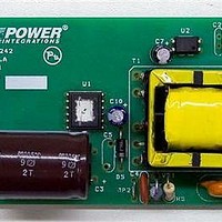
RDR-242 – 30 W Open Frame Supply using TOP266VG
load input power, from ~26 mW to ~10 mW. To compensate the resultant change in the
UV threshold resistor R12 was added between the CONTROL and VOLTAGE-MONITOR
pins. This adds a DC current equal to ~16 mA into the V pin, requiring only 9 A to be
provided via R1 and R2 to reach the V pin UV threshold current of 25 A and setting the
UV threshold to approximately 95 VDC.
This technique does effectively disable the line OV feature as the resultant OV threshold
is raised from ~450 VDC to ~980 VDC. However in this design there was no impact as
the value of input capacitance (C3) was sufficient to allow the design to withstand
differential line surges greater than 1 kV without the peak drain voltage reaching the
BV
rating of U1.
DSS
Specific guidelines and detailed calculations for the value of R12 may be found in the
TOPSwitch-JX Application Note AN-47.
4.1.4 Clamp Configuration – RZCD vs RCD
• An RZCD (Zener bleed) was selected over RCD to give higher light load efficiency and
lower no-load consumption
The clamp network is formed by VR1, C4, R5 and D5. It limits the peak drain voltage
spike caused by leakage inductance to below the BV
rating of the internal
DSS
TOPSwitch-JX MOSFET. This arrangement was selected over a standard RCD clamp to
improve light load efficiency and no-load input power.
In a standard RCD clamp C4 would be discharged by a parallel resistor rather than a
resistor and series Zener. In an RCD clamp the resistor value of R5 is selected to limit
the peak drain voltage under full load and over-load conditions. However under light or
no-load conditions this resistor value now causes the capacitor voltage to discharge
significantly as both the leakage inductance energy and switching frequency are lower.
As the capacitor has to be recharged to above the reflected output voltage each
switching cycle the lower capacitor voltage represents wasted energy. It has the effect of
making the clamp dissipation appear as a significant load just as if it were connected to
the output of the power supply.
The RZCD arrangement solves this problem by preventing the voltage across the
capacitor discharging below a minimum value (defined by the voltage rating of VR1) and
therefore minimizing clamp dissipation under light and no-load conditions. Zener VR1 is
shown as a high peak dissipation capable TVS however a standard lower cost Zener may
also be used due to the low peak current that component experiences.
In many designs a resistor value of less than 50 may be used in series with C4 to
damp out high frequency ringing and improve EMI but this was not necessary in this
case.
Power Integrations
Tel: +1 408 414 9200 Fax: +1 408 414 9201
Page 9 of 59
www.powerint.com
Related parts for RDK-242
Image
Part Number
Description
Manufacturer
Datasheet
Request
R

Part Number:
Description:
KIT REF DESIGN TOP HX FOR TOP258
Manufacturer:
Power Integrations
Datasheet:

Part Number:
Description:
KIT REF DESIGN LINKSWITCH 2
Manufacturer:
Power Integrations
Datasheet:

Part Number:
Description:
KIT REF DESIGN 1.2W PS TN FAMILY
Manufacturer:
Power Integrations
Datasheet:

Part Number:
Description:
KIT REF DESIGN 36-72W MOTOR DRVR
Manufacturer:
Power Integrations
Datasheet:

Part Number:
Description:
KIT REF DESIGN FOR LNK457D
Manufacturer:
Power Integrations
Datasheet:

Part Number:
Description:
REFERENCE DESIGN LINKSWITCH-PH
Manufacturer:
Power Integrations
Datasheet:

Part Number:
Description:
Specifications: Manufacturer: Power Integrations ; Output Voltage: 380 VDC ; Input / Supply Voltage (Max): 264 VAC ; Input / Supply Voltage (Min): 90 VAC ; Mounting Style: Through Hole ; Output Current: 0.913 A ; Output Power: 347 W
Manufacturer:
Power Integrations, Inc.
Part Number:
Description:
Power Management IC Development Tools REF DESIGN RDR-292 PFF LED STREET LIGHT
Manufacturer:
Power Integrations

Part Number:
Description:
KIT REF DESIGN FOR LNK403EG
Manufacturer:
Power Integrations
Datasheet:

Part Number:
Description:
KIT REF DESIGN FOR LNK406EG
Manufacturer:
Power Integrations
Datasheet:

Part Number:
Description:
KIT REF DESIGN DG CAPZERO
Manufacturer:
Power Integrations
Datasheet:

Part Number:
Description:
KIT REF DESIGN LINKSWITCH-CV
Manufacturer:
Power Integrations
Datasheet:

Part Number:
Description:
KIT REF DESIGN PFS762HG
Manufacturer:
Power Integrations
Datasheet:
Part Number:
Description:
Specifications: Family: Eval Boards - DC/DC & AC/DC (Off-Line) SMPS ; Series: HiperLCS™ ; Main Purpose: DC/DC, Step Down ; Outputs and Type: 1, Isolated ; Power - Output: 150W ; Voltage - Output: 24V ; Current - Output: 6.25A ; Voltage - Input:
Manufacturer:
Power Integrations, Inc.
Datasheet:

Part Number:
Description:
KIT REFERENCE DESIGN W/TN376PN
Manufacturer:
Power Integrations
Datasheet: