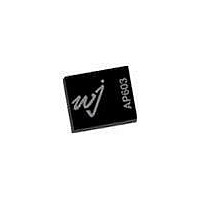
AP603-PCB900 TriQuint, AP603-PCB900 Datasheet - Page 14

AP603-PCB900
Manufacturer Part Number
AP603-PCB900
Description
RF Modules & Development Tools 869-960MHz Eval Brd 17dB Gain
Manufacturer
TriQuint
Datasheet
1.AP603-PCB2140.pdf
(14 pages)
Specifications of AP603-PCB900
Board Size
6 mm x 5 mm x 1 mm
Minimum Frequency
869 MHz
Minimum Operating Temperature
- 40 C
Supply Voltage (min)
28 V
Product
RF Development Tools
Maximum Frequency
960 MHz
Output Power
7 W
Supply Voltage (max)
80 V
Supply Current
246 mA
Maximum Operating Temperature
+ 85 C
For Use With/related Products
AP603
Lead Free Status / RoHS Status
Lead free / RoHS Compliant
Other names
1067337
WJ Communications, Inc • Phone 1-800-WJ1-4401 • FAX: 408-577-6621 • e-mail: sales@wj.com • Web site: www.wj.com, www.TriQuint.com
Thermal Specifications
Parameter
Thermal Resistance, Θ
Junction Temperature, T
Max Junction Temperature, T
Referenced from peak junction to the
center of the bottomside ground paddle
For 10
For catastrophic failure
This package is lead-free and RoHS-compliant. It is compatible with both lead-free (maximum 260 °C reflow temperature) and leaded
6
(maximum 245 °C reflow temperature) soldering processes. The plating material on the pins is annealed matte tin over copper.
hours MTTF
AP603
High Dynamic Range 7W 28V HBT Amplifier
Mounting Configuration / Land Pattern
JC
J
J,max
Outline Drawing
Rating
8.7 °C / W
192 ºC
250 ºC
AP603-F Mechanical Information
1.E+09
1.E+08
1.E+07
1.E+06
1.E+05
120
Drawing
MTTF vs. Junction Temperature
Junction Temperature (°C)
140
160
180
200
Specifications and information are subject to change without notice
The component will be laser marked with an
“AP603-F” product label with an alphanumeric
lot code on the top surface of the package.
Tape and reel specifications for this part will be
located on the website in the “Application
Notes” section.
ESD Rating: Class 1B
Value:
Test:
Standard:
ESD Rating: Class IV
Value:
Test:
Standard:
MSL Rating: Level 3 at +260 °C convection reflow
Standard:
Functional Pin Layout
Backside paddle
2, 3, 7, 8, 12, 13
MSL / ESD Rating
Product Marking
9, 10, 11
4, 5, 6
Passes
Human Body Model (HBM)
JEDEC Standard JESD22-A114
Passes
Charged Device Model (CDM)
JEDEC Standard JESD22-C101
JEDEC Standard J-STD-020
Pin
14
1
500V to <1000V
1000V to <2000V
RF Output / Vcc
Page 14 of 14 May 2007 ver 1
PIN_VBIAS
PIN_VPD
Function
RF IN
GND
N/C


