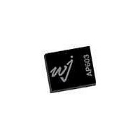
AP603-PCB900 TriQuint, AP603-PCB900 Datasheet - Page 5

AP603-PCB900
Manufacturer Part Number
AP603-PCB900
Description
RF Modules & Development Tools 869-960MHz Eval Brd 17dB Gain
Manufacturer
TriQuint
Datasheet
1.AP603-PCB2140.pdf
(14 pages)
Specifications of AP603-PCB900
Board Size
6 mm x 5 mm x 1 mm
Minimum Frequency
869 MHz
Minimum Operating Temperature
- 40 C
Supply Voltage (min)
28 V
Product
RF Development Tools
Maximum Frequency
960 MHz
Output Power
7 W
Supply Voltage (max)
80 V
Supply Current
246 mA
Maximum Operating Temperature
+ 85 C
For Use With/related Products
AP603
Lead Free Status / RoHS Status
Lead free / RoHS Compliant
Other names
1067337
WJ Communications, Inc • Phone 1-800-WJ1-4401 • FAX: 408-577-6621 • e-mail: sales@wj.com • Web site: www.wj.com, www.TriQuint.com
Typical WCDMA Performance at 25 °C
Frequency
W-CDMA Channel Power
Power Gain
Input Return Loss
Output Return Loss
ACLR
IMD3 @ +30 dBm PEP
Operating Current, Icc
Collector Efficiency
Output P1dB
Quiescent Current, Icq
Vpd, Vbias
Vcc
18
17
16
15
14
13
-40
-45
-50
-55
-60
-65
at a channel power of +30 dBm
30
22
920 MHz
940 MHz
960 MHz
ACLR1 vs. Output Power vs. Frequency
920 MHz
940 MHz
960 MHz
AP603
High Dynamic Range 7W 28V HBT Amplifier
Gain vs. Output Power vs. Frequency
32
24
Average Output Power (dBm)
CW tone, Vcc = 28V, Icq = 160 mA, 25 ˚C
WCDMA, Vcc = 28V, Icq = 160 mA, 25 ˚C
L3
Output Power (dBm)
W-CDMA 3GPP Test Model 1+64 DPCH, 60% clipping, PAR = 8.6 dB @ 0.01% Probability, 3.84 MHz BW
C5
34
26
920-960 MHz Application Circuit Performance Plots
920-960 MHz Application Circuit (AP603-PCB900)
36
28
+38.5 dBm
940 MHz
+30 dBm
217 mA
160 mA
-52 dBc
-52 dBc
38
30
16.6 %
5.5 dB
17 dB
+28 V
11 dB
+5 V
40
32
-10
-15
-20
-25
-50
-55
-60
-65
-70
-75
-5
0
0.8
Notes:
1. The primary RF microstrip line is 50 Ω.
2. Components shown on the silkscreen but not on the schematic are not used.
3. The center of C24 is placed at 0.245” (10.0° @ 940 MHz) from the center of C5.
4. The center of C5 is placed at .060” (2.5° @ 940 MHz) from the edge of the AP603 (U1).
5. The center of L4 is placed at 0.170” (7.0° @ 940 MHz) from the edge of the AP603 (U1). L4
6. The center of C25 is placed at 0.480” (19.7° @ 940 MHz) from the center of L4.
7. The bold-faced RF trace is for the DC bias feed. The stub’s length is approximately a ¼ λ.
8. The main RF trace is cut at component L3 and L4 for this particular reference design.
26
CW 2-tone signal, 940 MHz, ∆f = 1 MHz, 28V, 160 mA Icq, 25 ˚C
is required to be an AVX 0805 type.
S11
S22
0.85
28
Output Power, PEP (dBm)
S11, S22 vs. Frequency
Vcc = 28V, Icq = 160 mA, 25 ˚C
0.9
IMD vs. Output Power
Frequency (GHz)
30
5.6pF
See note 3
0.95
1.8 Ohm
32
1
1.05
34
IMD3L
IMD3U
IMD5
1.1
See note 4
36
Specifications and information are subject to change without notice
1000pF
C7
50
40
30
20
10
25
20
15
10
0
5
0
14
22
920 MHz
940 MHz
960 MHz
Efficiency vs. Output Power vs. Frequency
Efficiency vs. Output Power vs. Frequency
920 MHz
940 MHz
960 MHz
18
24
Average Output Power (dBm)
CW tone, Vcc = 28V, Icq = 160 mA, 25 ˚C
WCDMA, Vcc = 28V, Icq = 160 mA, 25 ˚C
See note 5
Output Power (dBm)
22
26
26
Page 5 of 14 May 2007 ver 1
28
30
See note 6
30
34
38
32


