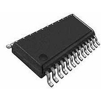
WM8731SEDS/V Wolfson Microelectronics, WM8731SEDS/V Datasheet - Page 34

WM8731SEDS/V
Manufacturer Part Number
WM8731SEDS/V
Description
Audio CODECs Stereo Codec with H/P
Manufacturer
Wolfson Microelectronics
Datasheet
1.WM8731LSEFLR.pdf
(64 pages)
Specifications of WM8731SEDS/V
Interface Type
Serial (2-Wire or 3-Wire), I2S
Resolution
24 bit
Operating Supply Voltage
2.7 V to 3.6 V
Maximum Operating Temperature
+ 85 C
Mounting Style
SMD/SMT
Package / Case
SSOP-28
Minimum Operating Temperature
- 40 C
Number Of Channels
2 ADC / 2 DAC
Snr
90 dB
Thd Plus Noise
- 84 dB
Lead Free Status / RoHS Status
Lead free / RoHS Compliant
WM8731 / WM8731L
w
DEVICE OPERATION
The side tone mode and attenuation is selected under software control using the SIDETONE bit as
shown in Table 11. In true side tone the output from the DAC (DACSEL) and line inputs (BYPASS)
should be deselected from the line output block. However, this can also be used to sum the DAC
output, line inputs and microphone inputs together.
headphone output volume control and mutes are still operational in side tone mode. The maximum
signal at any point in the side tone path must be no greater than 1.0V rms at VDD = 3.3V, to avoid
distortion. This amplitude tracks linearly with AVDD.
DEVICE RESETTING
The WM8731/L contains a power on reset circuit that resets the internal state of the device to a
known condition. The power on reset is applied as DCVDD powers on and released only after the
voltage level of DCVDD crosses a minimum turn off threshold. If DCVDD later falls below a minimum
turn on threshold voltage then the power on reset is re-applied. The threshold voltages and
associated hysteresis are shown in the Electrical Characteristics table.
The user also has the ability to reset the device to a known state under software control as shown in
the table below.
Table 12 Software Control of Reset
When using the software reset. In 3-wire mode the reset is applied on the rising edge of CSB and
released on the next rising edge of SCLK. In 2-wire mode the reset is applied for the duration of the
ACK signal (approximately 1 SCLK period, refer to Figure 34).
CLOCKING SCHEMES
In a typical digital audio system there is only one central clock source producing a reference clock to
which all audio data processing is synchronised. This clock is often referred to as the audio system’s
Master Clock. To allow WM8731/L to be used in a centrally clocked system, the WM8731/L is
capable of either generating this system clock itself or receiving it from an external source as will be
discussed.
For applications where it is desirable that the WM8731/L is the system clock source, then clock
generation is achieved through the use of a suitable crystal connected between the XTI/MCLK input
and XTO output pins (see CRYSTAL OSCILLATOR section).
For applications where a component other than the WM8731/L will generate the reference clock, the
external system can be applied directly through the XTI/MCLK input pin with no software
configuration necessary. Note that in this situation, the oscillator circuit of the WM8731/L can be
safely powered down to conserve power (see POWER DOWN section).
CORE CLOCK
The WM8731/L DSP core can be clocked either by MCLK or MCLK divided by 2. This is controlled by
software as shown in Table 13 below.
Table 13 Software Control of Core Clock
Having a programmable MCLK divider allows the device to be used in applications where higher
frequency master Clocks are available. For example the device can support 512fs master clocks
whilst fundamentally operating in a 256fs mode.
0001111
Reset Register
0001000
Sampling
Control
REGISTER
ADDRESS
REGISTER
ADDRESS
6
BIT
8:0
BIT
CLKIDIV2
RESET
LABEL
LABEL
0
DEFAULT
not reset
DEFAULT
The microphone boost gain control and
Reset Register
Writing 00000000 to register resets
device
1 = Core Clock is MCLK divided by 2
0 = Core Clock is MCLK
Core Clock divider select
DESCRIPTION
DESCRIPTION
PD, Rev 4.8, April 2009
Production Data
34


