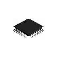
ispPAC-CLK5610AV-01TN48C Lattice, ispPAC-CLK5610AV-01TN48C Datasheet - Page 51

ispPAC-CLK5610AV-01TN48C
Manufacturer Part Number
ispPAC-CLK5610AV-01TN48C
Description
Clock Drivers & Distribution ISP 0 Dlay Clck Gen w/Unv Fan-Out Buf I
Manufacturer
Lattice
Type
Zero Delay Programmable PLL Clock Generatorr
Datasheet
1.ISPPAC-CLK5610AV-01TN48I.pdf
(51 pages)
Specifications of ispPAC-CLK5610AV-01TN48C
Max Input Freq
400 MHz
Minimum Operating Temperature
0 C
Mounting Style
SMD/SMT
Supply Voltage (max)
3.6 V
Supply Voltage (min)
3 V
Maximum Operating Temperature
+ 70 C
Package / Case
TQFP-48
Lead Free Status / RoHS Status
Lead free / RoHS Compliant
Available stocks
Company
Part Number
Manufacturer
Quantity
Price
Company:
Part Number:
ISPPAC-CLK5610AV-01TN48C
Manufacturer:
Lattice Semiconductor Corporation
Quantity:
10 000
Part Number:
ISPPAC-CLK5610AV-01TN48C
Manufacturer:
LATTICE
Quantity:
20 000
Lattice Semiconductor
Revision History
March 2007
June 2008
Date
—
Version
01.3
01.4
—
Previous Lattice releases.
Added min. and max. values to Timing Adders for I/O Modes table.
Added min. and max. values to PLL Bypass Mode operation table.
Added Phase Lock Detect feature description.
Added M-Divider and N-Divider Bypass feature description.
Modified logic standard related timing adder values in the Output Skew Matching Accu-
racy section and the Static Phase Offset and I/O Skew section.
PFD frequency limitation for the Static Phase Offset specification is removed.
Minimum operating voltage for V
Updated the I
Restructured / reordered sections under "Detailed Description" and "Thermal Manage-
ment"
Added a paragraph describing RESET in the "M-Divider and N-Divider Bypass Mode" sec-
tion.
Clairified the need for resetting ispClock in the “RESET and Power-up Functions” section.
CCD
vs. F
VCO
1-51
graph to include 800 MHz VCO frequency operation.
CCJ
Change Summary
is set to 2.25V.
ispClock5600A Family Data Sheet


