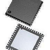
ASD5010L500INT Arctic Silicon Devices, ASD5010L500INT Datasheet - Page 30

ASD5010L500INT
Manufacturer Part Number
ASD5010L500INT
Description
ADC (A/D Converters) A-D Conv, Dig Gain Dual 8 bit 500MSPS
Manufacturer
Arctic Silicon Devices
Datasheet
1.ASD5010L500INT.pdf
(35 pages)
Specifications of ASD5010L500INT
Number Of Converters
2
Number Of Adc Inputs
4
Conversion Rate
500 MSPs
Resolution
8 bit
Snr
49.5 dB
Voltage Reference
1 V
Supply Voltage (max)
2 V
Supply Voltage (min)
1.7 V
Maximum Power Dissipation
295 mW
Maximum Operating Temperature
+ 85 C
Mounting Style
SMD/SMT
Package / Case
QFN-48
Input Voltage
1.8 V
Minimum Operating Temperature
- 40 C
Lead Free Status / RoHS Status
Lead free / RoHS Compliant
Preliminary Product Specification
Analog Input Invert
The IPx pin represents the positive analog input pin, and INx represents the negative (complementary) input. Setting the
bits marked invertx_ch<n:1> (individual control for each channel) causes the inputs to be swapped. INx would then
represent the positive input, and IPx the negative input.
LVDS Test Patterns
To ease the LVDS synchronization setup of ASD5010, several test patterns can be set up on the outputs. Normal ADC
data are replaced by the test pattern in these modes. Setting en_ramp to '1' sets up a repeating full-scale ramp pattern
on all data outputs. The ramp starts at code zero and is increased 1LSB every clock cycle. It returns to zero code and
starts the ramp again after reaching the full-scale code.
A constant value can be set up on the outputs by setting single_custom_pat to '1', and programming the desired value in
bits_custom1<7:0>. In this mode, bits_custom1<7:0> replaces the ADC data at the output, and is controlled by LSB-first
and MSB-first modes in the same way as normal ADC data are.
The device may also be made to alternate between two codes by programming dual_custom_pat to '1'. The two codes
are the contents of bits_custom1<7:0> and bits_custom2<7:0>.
Two preset patterns can also be selected:
Note: Only one of the above patterns should be selected at the same time.
ASD5010
invert4_ch<4:1>
invert2_ch<2:1>
invert1_ch1
en_ramp
dual_custom_pat
single_custom_pat
bits_custom1
<7:0>
bits_custom2
<7:0>
pat_deskew
pat_sync
1.
2.
Name
Name
Deskew pattern: Set using pat_deskew, this mode replaces the ADC output with '01010101'
Sync pattern: Set using pat_sync, the normal ADC word is replaced by a fixed '11110000' word
Channel specific swapping of the
analog input signal for a Quad
Channel setup.
Channel specific swapping of the
analog input signal for a Dual
Channel setup.
Channel specific swapping of the
analog input signal for a 1 channel
setup.
Enables a repeating full-scale ramp
pattern on the outputs.
Enable the mode wherein the output
toggles between two defined codes.
Enables the mode wherein the output
is a constant specified code.
Bits for the single custom pattern and
for the first code of the dual custom
pattern. <0> is the LSB.
Bits for the second code of the dual
custom pattern.
Enable deskew pattern mode.
Enable sync pattern mode.
Description
Description
IPx is positive input
IPx is positive input
IPx is positive input
rev 2.0, 2010.11.08
Default
Default
Inactive
Inactive
Inactive
Inactive
Inactive
Page 30 of 35
0x00
0x00
D15 D14D13D12D11D10 D9 D8 D7 D6 D5 D4 D3 D2 D1 D0
D15 D14D13D12D11D10 D9 D8 D7 D6 D5 D4 D3 D2 D1 D0
X
X
X
X
X
X
X
X
X
X
X X X
X X X
X
X 0 0
0 X 0
0 0 X
X X
X X X X
0 X
X 0
Confidential
Address
Address
0x24
0x25
0x26
0x27
0x45
Hex
Hex


